Semiconductor device and method of manufacturing the same

A semiconductor and device technology, applied in the field of semiconductor devices and their manufacturing, can solve the problems of increased cost, increased number of semiconductor device components, design changes, increased number of assembly steps, etc., and achieve the effect of improved manufacturing efficiency

Active Publication Date: 2012-09-26
SOCIONEXT INC
View PDF9 Cites 9 Cited by
  • Summary
  • Abstract
  • Description
  • Claims
  • Application Information

AI Technical Summary

Problems solved by technology

However, the fabrication of these shielding members or heat sinks may result in an increase in the number of parts of the semiconductor dev

Method used


Image

  • Semiconductor device and method of manufacturing the same
  • Semiconductor device and method of manufacturing the same
  • Semiconductor device and method of manufacturing the same

Examples


no. 1 example

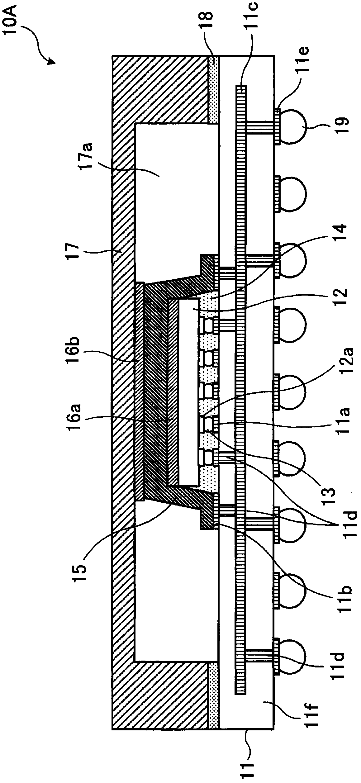
[0040] A first embodiment will now be described. figure 1 An example semiconductor device according to the first embodiment is shown.

[0041] A semiconductor device 10A according to the first embodiment includes a substrate (wiring board) 11 and semiconductor elements (semiconductor chips) 12 arranged on the substrate 11 .

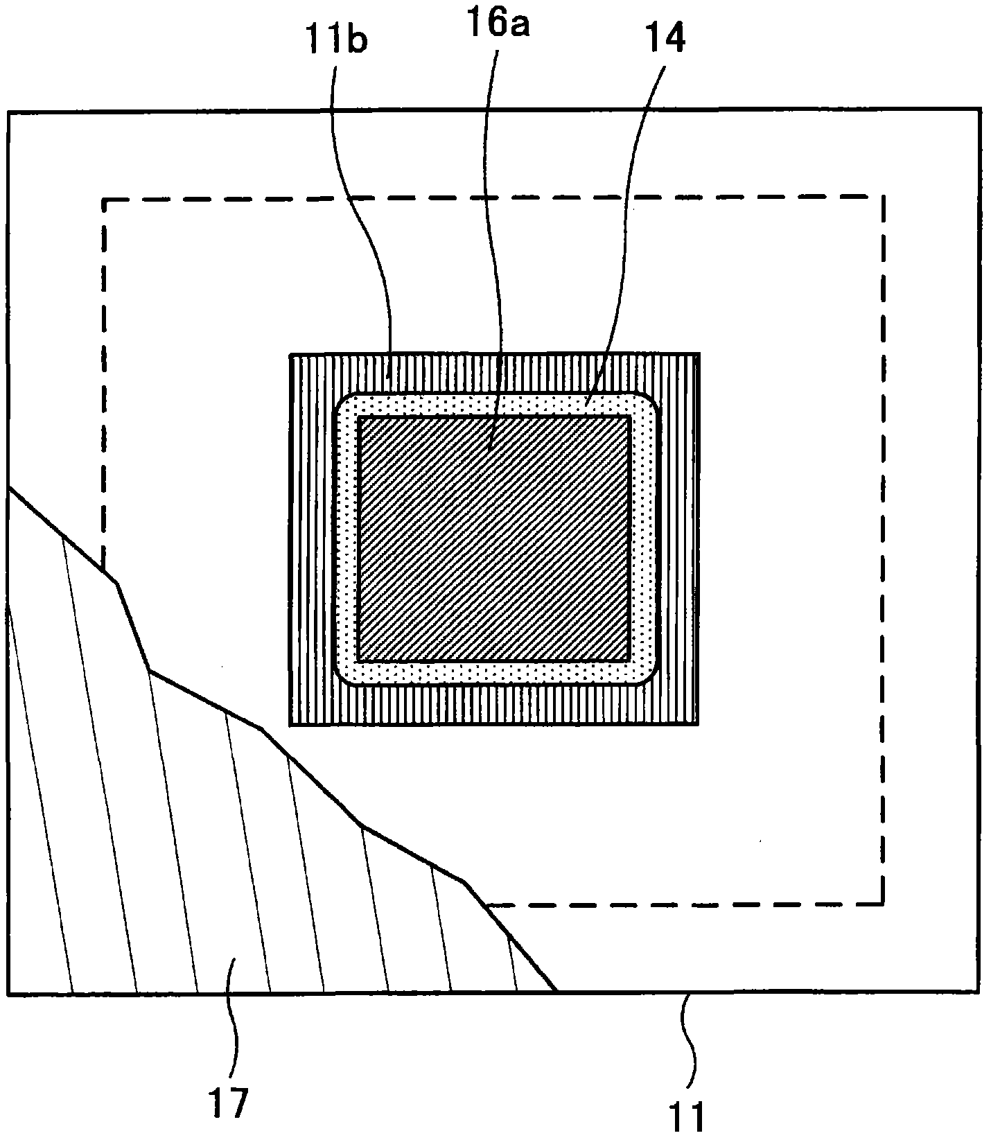
[0042] The substrate 11 has an electrode portion (substrate electrode pad) 11 a arranged on a surface opposite to the semiconductor element 12 . The substrate electrode pad 11a is electrically connected to an internal wiring 11c at a ground (GND) potential and a signal line (not shown) arranged inside the substrate 11 through a via 11d.

[0043] The semiconductor element 12 has an electrode portion (chip electrode pad) 12a arranged on a surface opposite to the substrate 11 at a position corresponding to the substrate electrode pad 11a. The semiconductor element 12 is mounted (flip-chip mounted) on the substrate 11 via the chip electrode pad 12a connecte...

no. 2 example

[0105] A second embodiment will now be described. Figure 14A and Figure 14B An example semiconductor device according to the second embodiment is shown. Figure 14A is along Figure 14B A schematic cross-sectional view taken along the midline L8-L8, Figure 14B is a schematic floor plan.

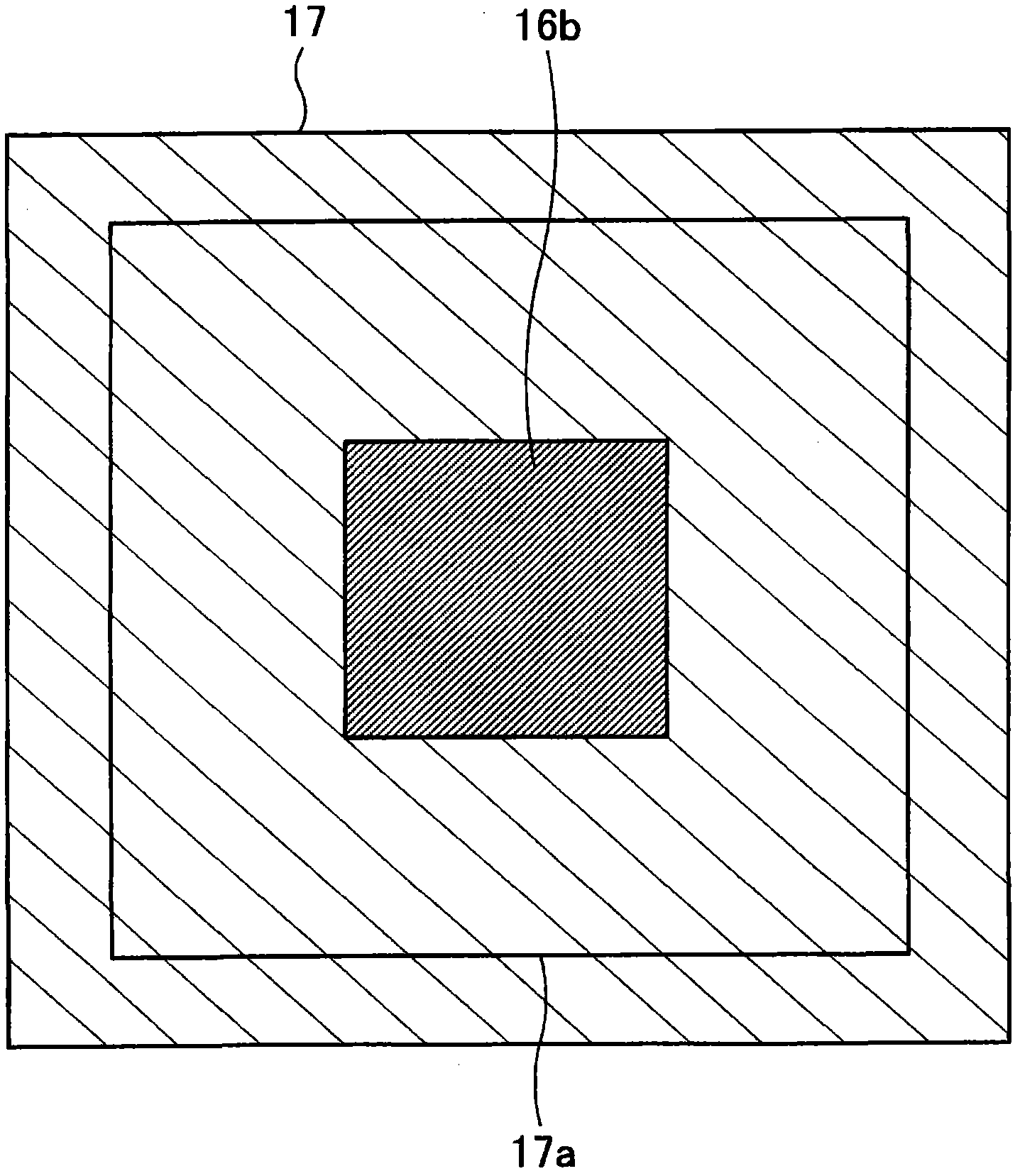
[0106] A semiconductor device 10B according to the second embodiment differs from the semiconductor device 10A according to the first embodiment in that the semiconductor device 10B includes a small-sized substrate 11 and a small-sized plate-shaped radiator 17 .

[0107] In the semiconductor device 10B, unlike the semiconductor device 10A according to the first embodiment, the heat sink 17 does not need to have a structure surrounding the periphery of the semiconductor element 12 and to be connected to the substrate 11 , that is, the concave portion 17 a. Due to the use of such a small plate-shaped heat sink 17, the substrate 11 does not need to have an area to which the heat sink 17 i...

no. 3 example

[0113] A third embodiment will now be described. Figure 15A and Figure 15B An example semiconductor device according to the third embodiment is shown. Figure 15A is along Figure 15B A schematic cross-sectional view taken along the midline L9-L9, Figure 15B is a schematic floor plan.

[0114] A semiconductor device 10C according to the third embodiment differs from the semiconductor device 10B according to the second embodiment in that the semiconductor device 10C includes a heat conduction member 15 having an opening 15c. The opening 15 c of the heat conduction member 15 can be used for application of an underfill resin 14 (described later).

[0115] A method of forming the semiconductor device 10C including the heat conduction member 15 having the opening 15c will now be described.

[0116] Figure 16A and Figure 16B Example substrate preparation steps according to the third embodiment are shown. Figure 16A is along Figure 16B A schematic cross-sectional view t...


PUM


Abstract

The invention provides a semiconductor device and method of manufacturing the same. A semiconductor device includes a substrate, a semiconductor element disposed on the substrate, and a heat conductive member composed of a solder material. The heat conductive member covers the semiconductor element, and is connected to a connection pad formed on the substrate. A heat radiator is disposed on the heat conductive member. The heat conductive member thermally connecting the semiconductor element to the heat radiator reduces the risk that electromagnetic noise may be emitted from or may be incident on the semiconductor element.

Description

technical field [0001] Embodiments discussed herein relate to semiconductor devices and methods of manufacturing the same. Background technique [0002] In some techniques, a heat radiator such as a heat spreader, a heat sink, and a radiator cap thermally connected to the semiconductor element (the distance between the heat sink and the semiconductor element) is used. A heat conduction member is interposed therebetween) to dissipate heat generated at semiconductor elements included in the semiconductor device. From the viewpoint of reducing the risk of semiconductor element failure due to electromagnetic noise, a shielding member may be arranged around the semiconductor element, or a heat sink such as a heat sink and a radiator cover may be used as a shielding member (see, for example, Japanese Patent Patent Publication Nos. 2009-105366, 2002-158317, and 2005-026373 and Japanese National Publication No. 2006-510235 of International Patent Application). [0003] A shielding...

Claims


Application Information

Patent Timeline
IPC IPC(8): H01L23/552H01L23/367H01L21/48H01L21/50
CPCH01L2924/01049H01L2924/01051H01L2924/10158H01L24/73H01L2224/32225H01L2924/19105H01L2924/1626H01L2224/73253H01L2924/01047H01L2224/16225H01L2924/3511H01L2224/27013H01L2924/01006H01L24/16H01L2924/15192H01L2924/01073H01L2924/01079H01L2924/15311H01L2924/16251H01L2924/01005H01L2924/0103H01L2924/01082H01L2224/73204H01L2924/01013H01L2224/92225H01L23/552H01L2924/014H01L2924/16151H01L2924/01023H01L2924/16152H01L2924/01029H01L23/3675H01L24/32H01L2924/01033H01L2224/2612H01L2924/00012H01L21/4875H01L21/563H01L24/83
Inventor 井原匠
Owner SOCIONEXT INC
Why Eureka
Try Eureka