Antenna device

An antenna device and chip antenna technology, which can be applied to antenna grounding devices, antennas, antenna supports/installation devices, etc., can solve problems such as rising manufacturing costs and achieve the effect of widening the frequency band

Active Publication Date: 2012-09-26
MURATA MFG CO LTD
View PDF4 Cites 26 Cited by
  • Summary
  • Abstract
  • Description
  • Claims
  • Application Information

AI Technical Summary

Problems solved by technology

Therefore, when the antenna and the power supply line are integrated, the manufacturing cost tends to increase

Method used


Image

  • Antenna device
  • Antenna device
  • Antenna device

Examples


Embodiment Construction

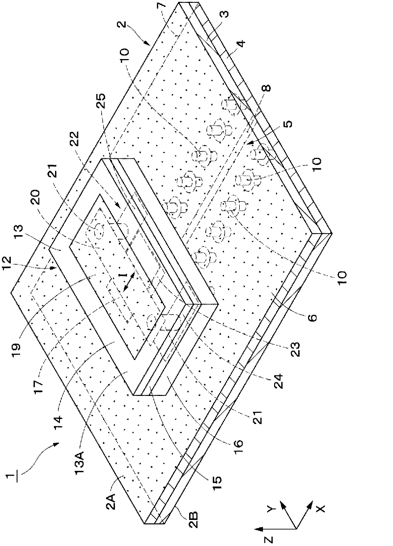
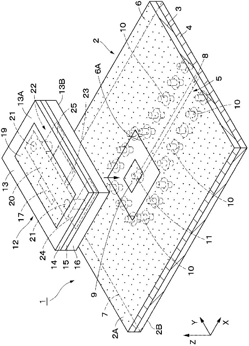
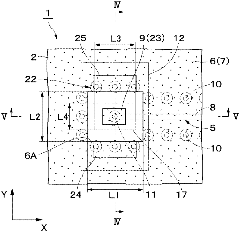
[0076] Hereinafter, a case where an antenna device according to an embodiment of the present invention is applied to a patch antenna for a 60 GHz band as an example will be described in detail with reference to the drawings.

[0077] Figure 1 to Figure 5 The antenna device 1 of the first embodiment is shown. This antenna device 1 is constituted by mounting a chip antenna 12 on a motherboard 2 described later.

[0078] The mother substrate 2 is formed in a flat plate shape extending parallel to, for example, the X-axis direction and the Y-axis direction among mutually orthogonal X-axis directions, Y-axis directions, and Z-axis directions. The motherboard 2 has a width of, for example, several millimeters with respect to the Y-axis direction serving as the width direction, a length dimension of, for example, several millimeters with respect to the X-axis direction serving as the longitudinal direction, and a length dimension of, for example, about several millimeters with resp...


PUM


Abstract

The invention provides an antenna device which is broadband adn can acquire expected antenna characteristics. A chip antenna is mounted on a mother substrate including a feed line. In a representative embodiment, the chip antenna includes a laminated body including plural insulating layers, a radiating conductor element, a parasitic conductor element, a coupling adjusting conductor plate, and a LGA. The radiating conductor element is connected to the feed line via a first flat electrode pad of the LGA. On the other hand, the coupling adjusting conductor plate is provided between the radiating conductor element and the parasitic conductor element, and both end sides of the coupling adjusting conductor plate are connected to second and third flat electrode pads of the LGA. Another representative embodiment does not include a coupling adjusting conductor plate in the laminated body and includes an LGA that may or may not include second and third flat electrode pads.

Description

technical field [0001] The present invention relates to an antenna arrangement suitable for high frequency signals such as microwave or millimeter wave. Background technique [0002] As a conventional antenna device, for example, there is known a microstrip (microstrip) antenna (patch antenna) in which radiating conductor elements and A ground conductor plate, and a non-power supply conductor element is provided on the radiation surface side of the radiation conductor element (for example, refer to Patent Document 1). [0003] 【Prior technical literature】 [0004] 【Patent Literature】 [0005] [Patent Document 1] Japanese Patent Application Laid-Open No. 55-93305 [0006] In addition, in the antenna device of Patent Document 1, wideband (bandwidth) is achieved by utilizing electromagnetic field coupling (coupling) of the radiating conductor element and the non-feeding conductor element. However, since the spacing dimension in the thickness direction between the radiating ...

Claims


Application Information

Patent Timeline
Patent Type & Authority Applications(China)
IPC IPC(8): H01Q1/38H01Q1/48H01Q1/12H01Q1/00
CPCH01Q9/0414H01Q1/00H01Q1/48H01Q1/38H01Q1/12
Inventor 藤井洋隆小林英一须藤薰平塚敏朗
Owner MURATA MFG CO LTD
Why Eureka
Try Eureka