Color filter substrate and manufacturing method for same

A technology for color filters and manufacturing methods, applied in the directions of filters, optics, optical components, etc., can solve the problems of lack of optical differentiation, low production efficiency and productivity, reduced equipment utilization rate, etc., to improve the position Calculate accuracy and equipment availability, improve production efficiency and productivity, and enhance the effect of optical differentiation

Inactive Publication Date: 2015-07-15
TCL CHINA STAR OPTOELECTRONICS TECH CO LTD
View PDF6 Cites 0 Cited by
  • Summary
  • Abstract
  • Description
  • Claims
  • Application Information

AI Technical Summary

Problems solved by technology

[0006] When using a CCD (Charge-coupled Device, charge-coupled device) optical reading lens to read the position of the alignment mark 1010, since the coverage characteristics of the transparent conductive layer 120 on the alignment mark 1010 and the peripheral area of ​​the alignment mark 1010 are the same , has no optical difference, so the success rate of the CCD optical reading lens in reading the alignment mark 1010 is not high, and even the reading fails, which causes the deviation of the position calculation accuracy of the process or reduces the utilization rate of the equipment , leading to low production efficiency and capacity

Method used


Image

  • Color filter substrate and manufacturing method for same
  • Color filter substrate and manufacturing method for same
  • Color filter substrate and manufacturing method for same

Examples


Embodiment Construction

[0028] The present invention will be described in further detail below in conjunction with the accompanying drawings and embodiments. The following examples are only used to illustrate the present invention, but should not be used to limit the scope of the present invention.

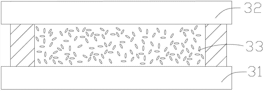
[0029] see image 3 , is a schematic structural view of a liquid crystal panel with a color filter substrate of the present invention. In this embodiment, the liquid crystal panel includes an active matrix substrate 31, a color filter substrate 32, and a substrate clamped between the active matrix substrate 31 and the color filter substrate. The liquid crystal layer 33 between the optical sheet substrates 32 .

[0030] The active matrix substrate 31 and the color filter substrate 32 are disposed opposite to each other, and include a transparent substrate, driving wiring and an alignment layer disposed on the transparent substrate. Since the active matrix substrate 31 used in the present invention is th...


PUM


Abstract

Provided are a liquid crystal display panel and a color filter substrate (32) and a manufacturing method thereof. The method comprises: forming a black matrix pattern (42, 52) in a pixel invalid area (401, 501) of a transparent substrate (40) to form a mark (42, 421, 52, 521); coating a transparent conductive layer (44, 441, 54, 541) on the pixel invalid area (401, 501) to cover the mark (42, 421, 52, 521); and performing patterning processing on the transparent conductive layer (44, 441, 54, 541), so that coverage characteristics of the transparent conductive layer (44, 441, 54, 541) are different at the mark (42, 421, 52, 521) and a peripheral zone of the mark (42, 421, 52, 521), thereby effectively enhancing the optical differences of the mark (42, 421, 52, 521) and the peripheral zone thereof under a CCD optical reading lens, improving the success rate of reading the mark (42, 421, 52, 521), and improving the production efficiency.

Description

technical field [0001] The invention relates to the technical field of liquid crystal display, in particular to a color filter substrate and a manufacturing method thereof. Background technique [0002] In the liquid crystal panel manufacturing process, the alignment mark (mark) plays an important role. When it is necessary to perform position confirmation and coordinate calculation, it is necessary to read the position of the alignment mark. For example, when performing coordinate positioning of precision measuring instruments and exposure alignment of exposure machines, it is necessary to read the position of the alignment marks; Confirm the group position of the substrate. [0003] see figure 1 , figure 1 It is a schematic diagram of setting the alignment mark on the existing color filter substrate. [0004] Such as figure 1 As shown, in the prior art, the transparent substrate 10 of the color filter substrate includes a plurality of effective pixel regions 100 and i...

Claims


Application Information

Patent Timeline
Patent Type & Authority Patents(China)
IPC IPC(8): G02F1/1335G02B5/20
CPCG02F1/133516G02B5/201G02B5/20G02F1/1335
Inventor 伍浚铭
Owner TCL CHINA STAR OPTOELECTRONICS TECH CO LTD
Why Eureka
Try Eureka