Method and system for exposing delicate structures of a device encapsulated in a mold compound

A control mechanism and laser beam technology, which is applied in manufacturing tools, welding/welding/cutting objects, semiconductor/solid-state device manufacturing, etc., can solve the problems of energy inconcentration, damage of sensitive IC components, IC chip damage, etc.

Inactive Publication Date: 2012-10-03
CONTROL LASER
View PDF4 Cites 3 Cited by
  • Summary
  • Abstract
  • Description
  • Claims
  • Application Information

AI Technical Summary

Problems solved by technology

However, if figure 2 It can be seen that the glass 20 inside the composite 24 of the IC 14 disperses the laser energy so that the energy is not concentrated which reduces the energy density to a point below the point where it is sufficient to ablate the composite
Raising the laser beam power to a level high enough to overcome the energy loss due to dispersion can result in the destruction of sensitive IC components at locations where the laser beam is not dispersed, destroying or damaging the IC chip to the point where failure analysis cannot be performed

Method used


Image

  • Method and system for exposing delicate structures of a device encapsulated in a mold compound
  • Method and system for exposing delicate structures of a device encapsulated in a mold compound
  • Method and system for exposing delicate structures of a device encapsulated in a mold compound

Examples


Embodiment Construction

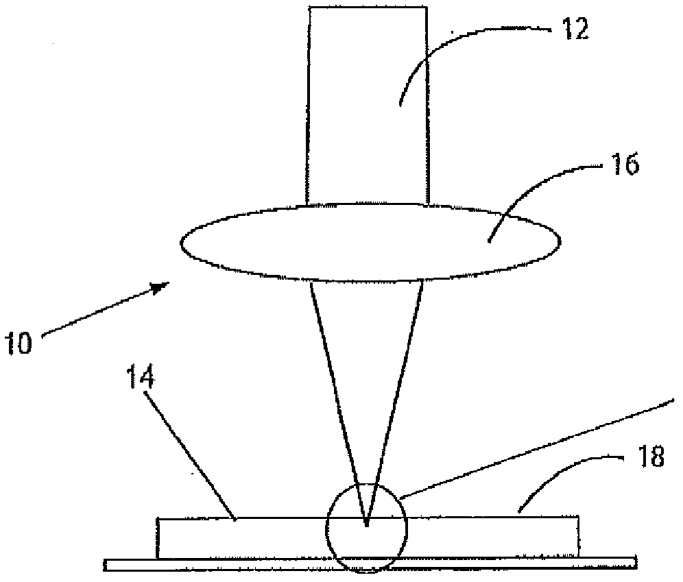
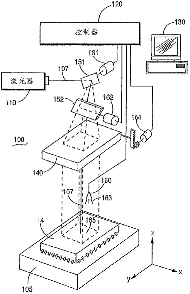
[0015] image 3 is a block diagram of an exemplary embodiment of a system 100 in accordance with the present invention. The device to be analyzed, such as an integrated circuit (IC) 14, is placed on a platform 105 where a laser beam 107 generated by a laser 110 is steered and focused by a pair of reflective blades 151 and 152 and a lens element 140 . Operation is controlled by a controller 120, which may be connected to a user interface 130 for human-computer interaction. For example, controller 120 and user interface 130 may be part of a workstation, personal computer, etc., or may be housed separately.

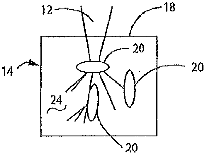
[0016] During operation, IC 14 remains stationary while light beam 107 is moved in a selective manner over selected portions of the IC surface. At any one time, laser beam 107 impinges on a point on the surface of IC 101 . To the naked eye, however, the laser beam looks like a straight line or a rectangle on the surface of the IC 101 , depending on how fast the laser bea...


PUM

PropertyMeasurementUnit
wavelengthaaaaaaaaaa

Abstract

A system utilizes a laser to remove the mold compound of an IC without damaging the internal die, wire leads, solder connections and any other critical structures encapsulated within the mold compound, thereby leaving them available for the provisional and electrical analysis. A laser beam is focused through appropriate optics onto a plane corresponding to the surface of an IC. A layer of material which is opaque at the wave length of the laser beam is applied at the surface of the IC chip to be ablated prior to each pass of the laser. A spray nozzle may be provided to move in synchronous motion ahead of the laser being to apply coat of the opaque material.

Description

[0001] Cross References to Related Applications [0002] This application claims priority under 35 U.S.C.111(a) to U.S. Utility Patent Application No. 12 / 580,652, filed October 16, 2009, entitled "METHOD AND SYSTEM FOR EXPOSING DELICATE STRUCTURES OF ADEVICE ENCAPSULATED IN AMOLD COMPOUNT" Interest, the disclosure of this application is incorporated herein by reference in its entirety. Background technique [0003] The present invention relates to methods and systems for utilizing ablative lasers for failure analysis in the manufacture of integrated circuits, and in particular to the manufacture of electrical devices or devices having components encapsulated in mold compounds containing glass or silicon impurities Circuits, methods and systems. [0004] The integrated circuit has failed. However, once an integrated circuit fails, it is often necessary to determine what caused the failure, which may trigger a product recall for corrective action. When analyzing a failure, ea...

Claims


Application Information

Patent Timeline
Patent Type & Authority Applications(China)
IPC IPC(8): H01L23/36H01L21/311
CPCB23K26/0807B23K26/18H01L21/56B23K26/1417B23K26/4085B23K26/1411B23K26/009B23K26/40B23K26/082B23K26/144B23K26/146B23K2103/16H01L2924/0002H01L2924/00
Inventor G·B·安德森
Owner CONTROL LASER
Why Eureka
Try Eureka