Semiconductor monocrystal silicon production process

A production process and technology of single crystal silicon, applied in the field of semiconductor-grade single crystal silicon production process, can solve the problems of difficult control of product quality, easy occurrence of vortex defects, poor uniformity of section resistivity, etc. The uniformity of section resistivity and the effect of speeding up production efficiency

Inactive Publication Date: 2012-10-10
XIAN HUAJING ELECTRONICS TECH
View PDF6 Cites 4 Cited by
  • Summary
  • Abstract
  • Description
  • Claims
  • Application Information

AI Technical Summary

Problems solved by technology

However, the semiconductor-grade monocrystalline silicon currently on the market has various defects and deficiencies such as poor uniformity of cross-sectional resistivity, easy occurrence of swirl defects, and difficult control of product quality.

Method used


Image

  • Semiconductor monocrystal silicon production process

Examples


Embodiment Construction

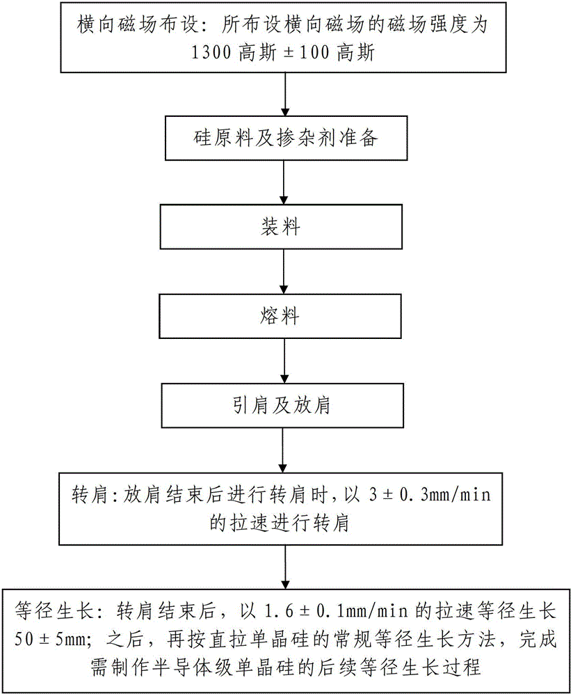
[0038] Such as figure 1 A semiconductor-grade monocrystalline silicon production process shown includes the following steps:

[0039] Step 1. Transverse magnetic field arrangement: a transverse magnetic field is arranged outside the middle part of the main furnace chamber 1 of the single crystal furnace that needs to produce semiconductor-grade single crystal silicon, and the magnetic field strength of the transverse magnetic field is 1300 Gauss ± 100 Gauss. Among them, 1 Gauss = 1 Oersted. It can also be said that the magnetic field strength of the transverse magnetic field is 1300 Oersted±100 Oersteds.

[0040] When the transverse magnetic field is actually laid out, the magnetic field strength of the transverse magnetic field is 1300 Gauss±20 Gauss. In this embodiment, the magnetic field strength of the transverse magnetic field is 1300 Gauss. During actual use, the magnetic field strength of the transverse magnetic field can be adjusted accordingly according to actual ne...


PUM

PropertyMeasurementUnit
magnetic flux densityaaaaaaaaaa

Abstract

The invention discloses a semiconductor monocrystal silicon production process, which includes the following steps: laying a transverse magnetic field with the intensity ranging from 1200 to 1400 G; preparing silicon raw materials and doping agent; loading materials; melting materials; shoulder leading and shouldering; shoulder rotating at the pull speed ranging from 2.7 to 3.3 mm/min after the shouldering; isodiametric growing for 45 to 55 mm at the pull speed ranging from 1.5 to 1.7 mm/min after the shoulder rotating; and completing the follow-up isodiametric growing process of the to-be-made semiconductor monocrystal silicon according to the ordinary isodiametric growing method of the straight-pulled monocrystal silicon. The semiconductor monocrystal silicon production process has reasonable design, simple method steps and excellent use effect, is convenient to realize and easy to master, can ensure the quality of the produced semiconductor monocrystal silicon, and enables the produced semiconductor monocrystal silicon to be highly uniform in the resistivity of the cross section and free from all sorts of microdefects as vortex formation.

Description

[0001] The patent application of the present invention is a divisional application of the invention patent application with the application date of July 15, 2011, the application number 201110199182.6, and the invention title "A Production Process for Semiconductor Grade Monocrystalline Silicon". technical field [0002] The invention belongs to the technical field of monocrystalline silicon production, and in particular relates to a semiconductor-grade monocrystalline silicon production process. Background technique [0003] Monocrystalline silicon, also known as monocrystalline silicon, is a semiconductor material. In recent years, with the rapid development of the photovoltaic industry, monocrystalline silicon has been used to make solar cells, showing a situation in which demand exceeds supply. With the development of high technology, it is the common wish of every material manufacturer and device manufacturer to produce nearly perfect high-quality single crystal silicon...

Claims


Application Information

Patent Timeline
Patent Type & Authority Applications(China)
IPC IPC(8): C30B15/20C30B29/06
Inventor 周建华
Owner XIAN HUAJING ELECTRONICS TECH
Why Eureka
Try Eureka