
Optical waveguide structure of photoelectric detector for vertical coupling

A vertical coupling, photodetector technology, applied in the direction of light guides, instruments, circuits, etc., to achieve the effects of low coupling loss, low coupling loss, and fast response speed

Inactive Publication Date: 2012-10-10
UNIV OF ELECTRONICS SCI & TECH OF CHINA
View PDF5 Cites 14 Cited by
  • Summary
  • Abstract
  • Description
  • Claims
  • Application Information

AI Technical Summary

Problems solved by technology

[0006] The purpose of the present invention is to overcome the defects in the prior art that when the air gap on the coupling layer changes, the coupling length and absorption length of the photodiode will change, and propose a photodetector for coupling in the vertical direction The optical waveguide structure

Method used


Image

  • Optical waveguide structure of photoelectric detector for vertical coupling
  • Optical waveguide structure of photoelectric detector for vertical coupling
  • Optical waveguide structure of photoelectric detector for vertical coupling

Examples


Embodiment Construction

[0016] The present invention will be further described below in conjunction with accompanying drawing and specific embodiment:

[0017] Such as Figure 4 and 5 As shown, the optical waveguide structure of the photodetector for coupling in the vertical direction includes an intrinsic layer 1, an absorbing layer 2, an upper waveguide layer 3, a gap layer 4, a lower waveguide layer 5, and a cover layer stacked sequentially from top to bottom 6 and a substrate 7, the gap layer 4 is used as a low-refractive-index coupling layer between the upper waveguide layer 3 and the lower waveguide layer 5, and the upper waveguide layer 3 and the lower waveguide layer 5 form a coupler in the vertical direction (equivalent to a photodiode coupled in the vertical direction) is used to make the light incident from the lower waveguide layer 5 gradually coupled to the upper waveguide layer 3 and make the light be absorbed by the absorption layer 2 while being transmitted in the upper waveguide lay...


PUM


Abstract

The invention relates to an optical waveguide structure of a photoelectric detector for vertical coupling. The structure comprises an intrinsic layer, an absorption layer, an upper waveguide layer, a clearance layer, a lower waveguide layer, a cover layer and a substrate which are sequentially stacked from top to bottom, wherein the clearance layer is used as a low-refractive index coupling layer between the upper waveguide layer and the lower waveguide layer; and a vertical coupler (equivalent to a vertically-coupled photoelectric diode) composed of the upper waveguide layer and the lower waveguide layer is used for realizing that the light enters from the lower waveguide layer and is gradually coupled to the upper waveguide layer and transmitted in the upper waveguide layer and the lower waveguide layer while being absorbed by the absorption layer. The structure provided by the invention has the beneficial effect of overcoming the defects that the coupling length and the absorption length are changed when the air clearance in the horizontally-coupled photoelectric diode structure changes and the photoetching corrosion processing technology is difficult.

Description

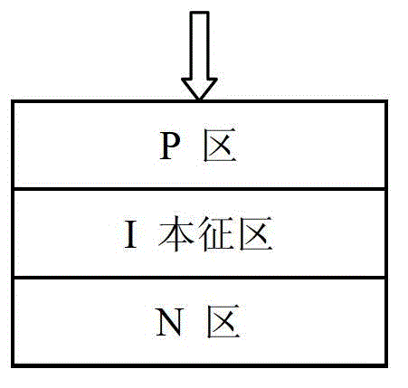
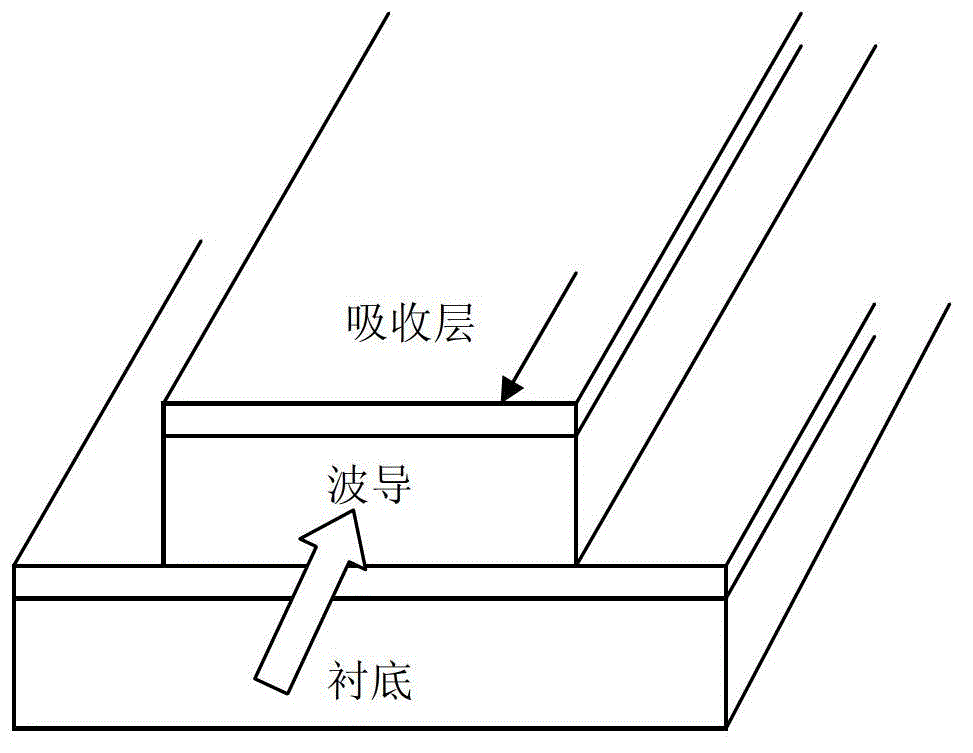
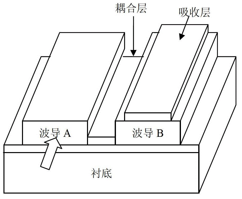
technical field [0001] The invention belongs to the field of optoelectronic technology, and in particular relates to a photodiode. Background technique [0002] Photodetectors are one of the indispensable devices in broadband communication systems, wireless communication systems and high-frequency measurement systems, and are also the core devices in optical receivers. A photodiode is an optical waveguide structure used in photodetectors for photoelectric conversion. The development of high-power and high-speed photodiodes began with an improvement on the traditional PIN (positive intrinsic negative diode) photodiode structure; the waveguide photodiode (Waveguide Diode, WD) scheme was proposed in the late 1990s and early 20th century; A directional coupling photodiode (Directional Coupling Photo Diode, DCPD) scheme was proposed. [0003] Such as figure 1 As shown, in the traditional PIN photodiode, the incident light is incident from the direction perpendicular to the PN ...

Claims


Application Information

Patent Timeline
Patent Type & Authority Applications(China)
IPC IPC(8): H01L31/0232G02B6/122H01L31/102
Inventor 余学才古燕西
Owner UNIV OF ELECTRONICS SCI & TECH OF CHINA
Learn More