Method, device, and system for controlling cache
A technology of high-speed buffering and control methods, which is applied in the computer field, can solve problems such as increasing waiting time, wasting bandwidth resources, and reducing CPU processing efficiency, so as to avoid synchronous work, avoid unnecessary synchronous work, and solve the problem of CPU waiting delay Effect
- Summary
- Abstract
- Description
- Claims
- Application Information
AI Technical Summary
Problems solved by technology
Method used
Image
Examples
Embodiment 1
[0024] The embodiment of the present invention firstly provides a cache memory control system. In order to make the description of the structure and principle of the system clearer, this embodiment describes the system by applying the system to a central processing unit CPU as an example.
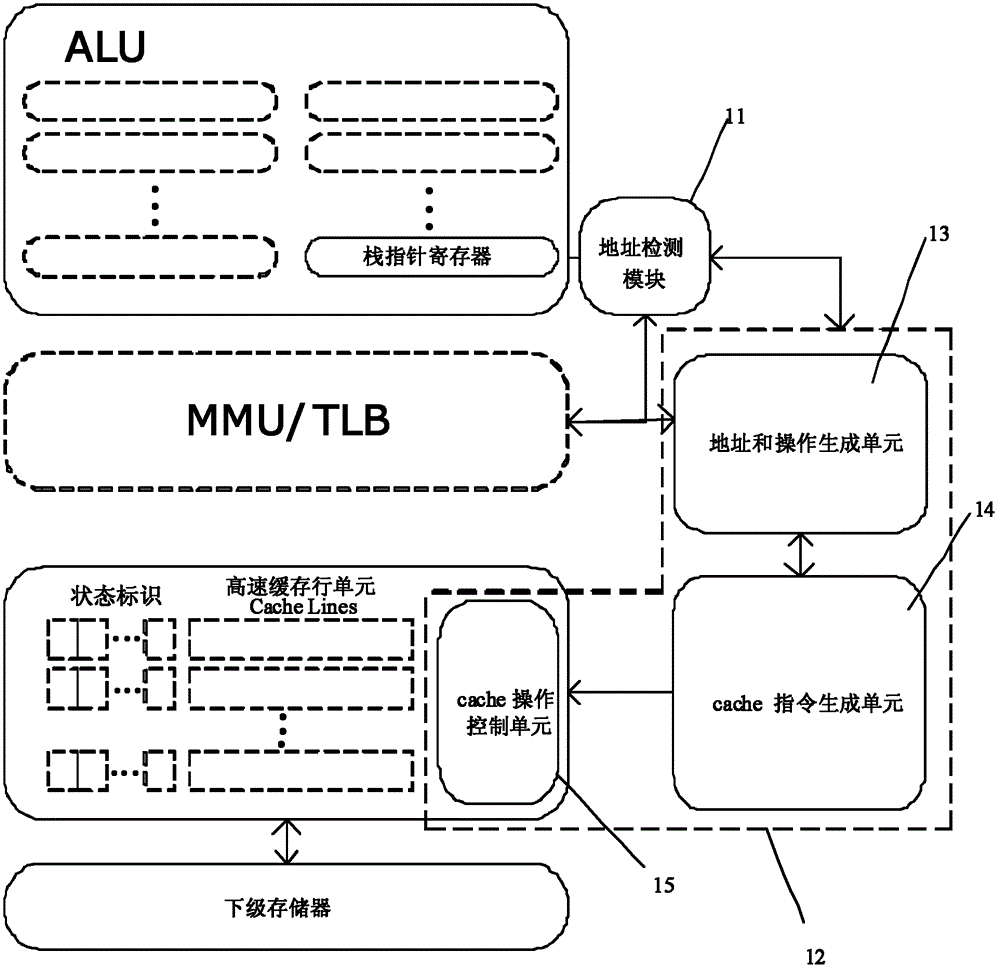
[0025] figure 1 It is a schematic diagram of the application structure of an embodiment of the cache memory control system of the present invention, such as figure 1 As shown, the system of this embodiment may include: an address detection module 11, a cache control module 12;
[0026] Wherein, the address detection module 11 is used to obtain the changed address range of the target object;
[0027] For example, the target object may include stack memory, heap memory, or memory for storing data such as code segments and data segments. The changed address range refers to, for example, for stack memory, the changed address range corresponds to the address range of stack growth or stack roll...
Embodiment 2
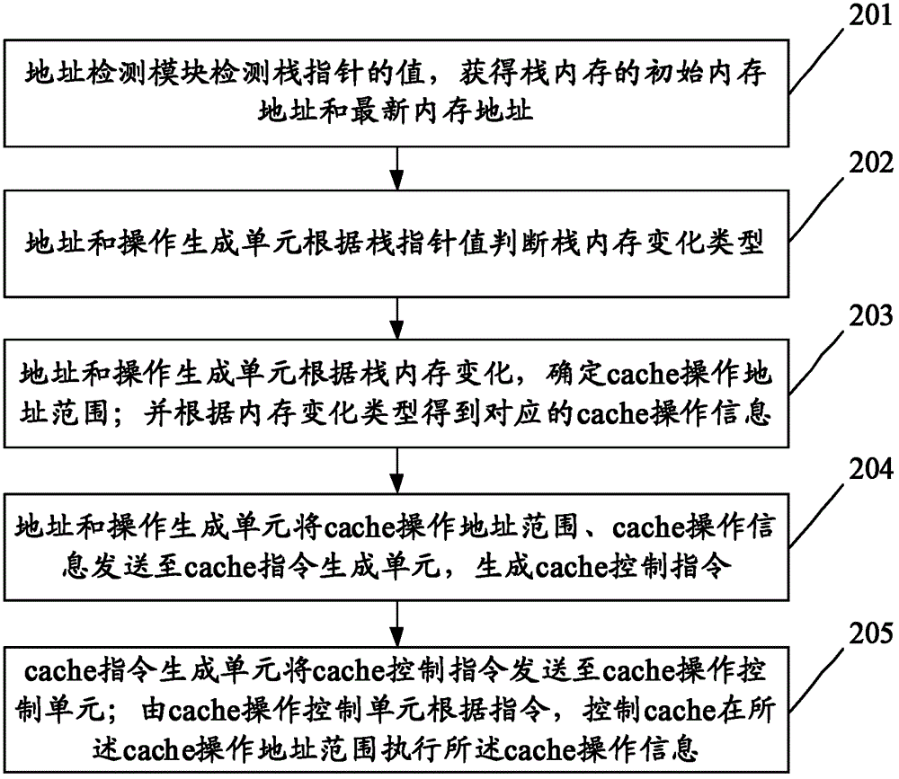
[0053] figure 2 It is a schematic diagram of the workflow of another embodiment of the cache memory control system of the present invention. This embodiment is a combination of figure 1 shown in the system structure, and the figure 2 In the system workflow shown, the working principle of the cache memory control system is explained by taking the cache control of stack growth and stack rollback as an example. Wherein, the present embodiment takes the example that there is no memory management unit (Memory Management Unit, MMU) in the CPU, that is, the format of the cache address and the detected memory address is consistent, and no virtual address (program memory address) is required. Address) to physical address (cache address) conversion.
[0054] 201. The address detection module detects the value of the stack pointer, and obtains the initial memory address and the latest memory address of the stack memory;
[0055] Wherein, the address of the stack memory is identified...
Embodiment 3
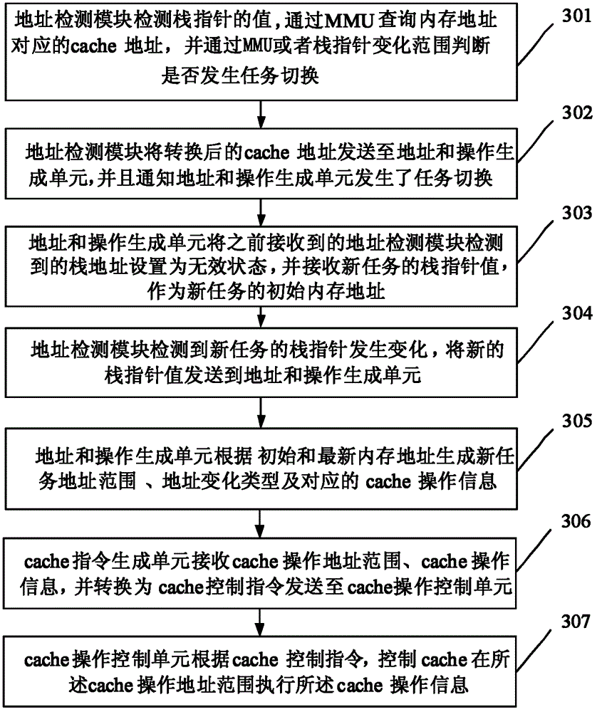
[0085] image 3 It is a schematic diagram of the workflow of another embodiment of the cache memory control system of the present invention, and this embodiment is the same as figure 2The difference of the illustrated embodiment is that there is an MMU in the applied CPU of the system of the present embodiment, and a conversion from a virtual address (memory address) to a physical address (cache address) is required; As an example, the task mentioned above refers to an application program, and switching refers to switching the program to another stack to run.
[0086] For example, if the value of the cr3 register of intel x86CPU changes, it means that the task is switched.
[0087] In addition, in the specific implementation, the translation lookaside buffer (Translation Lookaside Buffer, TLB for short) in the MMU can also be detected. By sending the virtual address of the stack pointer to the TLB, the TLB can convert the physical address. If the ASID in the hit TLBentry is ...
PUM
 Abstract
Description
Claims
Application Information


