Susceptor for supporting a semiconductor wafer and method for depositing a layer on a front side of a semiconductor wafer

A semiconductor and deposition layer technology, applied in semiconductor/solid-state device manufacturing, chemical instruments and methods, coatings, etc., to achieve the effect of small radial size

Inactive Publication Date: 2012-10-24
SILTRONIC AG
View PDF8 Cites 12 Cited by
  • Summary
  • Abstract
  • Description
  • Claims
  • Application Information

AI Technical Summary

Problems solved by technology

The disadvantage of the proposed solution is that, due to the uncontrolled deposition of material on the back side of the semiconductor wafer, the layers deposited on the front side up to the edge of the semiconductor wafer can therefore only be used to a limited extent.

Method used


Image

  • Susceptor for supporting a semiconductor wafer and method for depositing a layer on a front side of a semiconductor wafer
  • Susceptor for supporting a semiconductor wafer and method for depositing a layer on a front side of a semiconductor wafer
  • Susceptor for supporting a semiconductor wafer and method for depositing a layer on a front side of a semiconductor wafer

Examples


Embodiment Construction

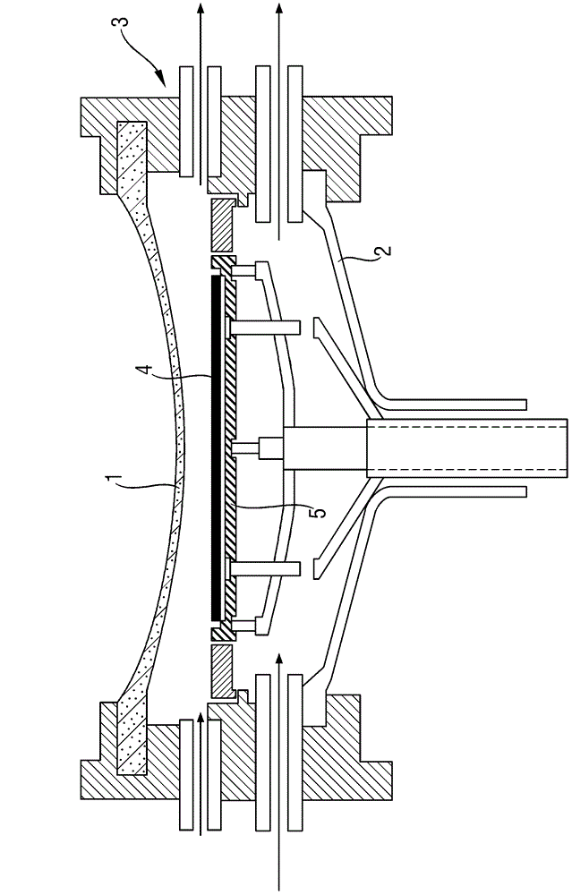
[0028] according to figure 1 The reactor comprises a chamber with an upper dome 1 , a lower dome 2 and side walls 3 . The upper dome 1 and the lower dome 2 are transparent to the thermal radiation emitted by the radiant heating system arranged above and below the chamber. The layer is deposited from the gas phase on the front side of the semiconductor wafer 4 by directing a process gas over the heated semiconductor wafer's front side and in the process reacting with the exposed front side surface to form the layer. Front side refers to the side of the semiconductor wafer on which the layers are deposited. Typically the polished side of a semiconductor wafer. The process gas is fed in through the gas inlet in the side wall of the chamber, and the waste gas remaining after the reaction is discharged through the gas outlet in the side wall of the chamber. Embodiments of chambers with one further gas inlet and one further gas outlet are known. These embodiments are employed, f...


PUM


Abstract

A susceptor for supporting a semiconductor wafer during deposition of a layer on a front side of the semiconductor wafer, the semiconductor wafer having a diameter D and, at its edge, a notch having a depth T, comprising: a ring-shaped placement area having an internal diameter d for the placement of the semiconductor wafer in the edge region of a rear side of the semiconductor wafer, wherein, with the semiconductor wafer having been placed, the relationship (D-d) / 2<T is satisfied,and a protrusion of the area for the placement of semiconductor wafer in the region of the notch of the semiconductor wafer extending the placement area inward, and which completely underlays the notch of the semiconductor wafer.

Description

technical field [0001] The invention relates to a susceptor for supporting a semiconductor wafer during deposition of a layer on the front side of the semiconductor wafer, wherein the susceptor has a placement area for placing the semiconductor wafer in the edge region of the back side of the semiconductor wafer. The invention also relates to a method for depositing a layer on the front side of a semiconductor wafer, wherein said susceptor is used. Background technique [0002] Various embodiments of such bases are known. DE 198 47 101 C1 describes an embodiment in which the placement area is part of a ring forming the base. In an embodiment according to EP 1 460 679 A1, the base additionally has a bottom and is thus disc-shaped. The placement area is constituted by a raised portion at the edge of the disc. DE 10 2006 055 038 A1 discloses an embodiment in which a semiconductor wafer is located in a recessed portion of a ring and the ring is located on a base plate. [00...

Claims


Application Information

Patent Timeline
Patent Type & Authority Applications(China)
IPC IPC(8): H01L21/673H01L21/02
CPCH01L21/68735C30B25/12C23C16/4585
Inventor N·维尔纳C·哈格尔R·绍尔
Owner SILTRONIC AG
Why Eureka
Try Eureka