

Method for manufacturing array substrate, array substrate and display device
An array substrate and substrate technology, which is used in semiconductor/solid-state device manufacturing, instruments, semiconductor devices, etc., can solve the problems of abnormal display of pixel electrodes 6, steep gradient angles of step differences, and defective pixel electrode faults, so as to solve abnormal display and avoid abnormal display. severing effect
- Summary
- Abstract
- Description
- Claims
- Application Information
AI Technical Summary
Problems solved by technology
Method used
Image

Examples
Embodiment 1
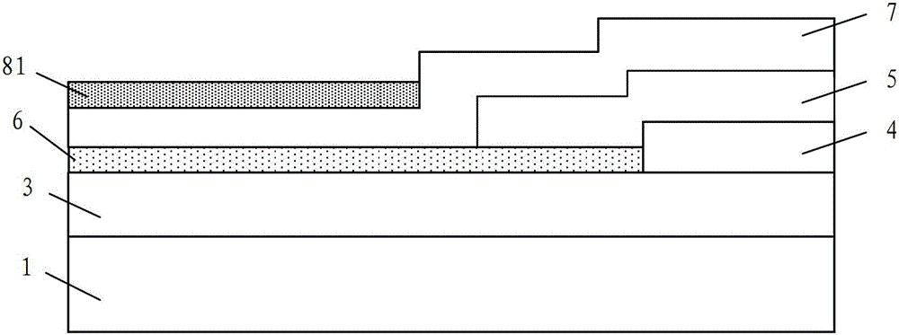
[0099] refer to image 3 , the array substrate of the embodiment of the present invention may include:
[0100] Substrate 1;
[0101] A gate electrode and a gate line formed by a gate metal layer on the substrate 1 (not shown in the figure);
[0102] a gate insulating layer 3 located on the substrate 1 formed with the gate electrode and the gate line;
[0103] an active layer 4 located on the gate insulating layer 3;
[0104] A source electrode (not shown in the figure), a drain electrode 5 and a data line (not shown in the figure) located on the active layer 4;
[0105] A pixel electrode 6 with a step portion 10 located on the substrate 1 formed with the source electrode, the drain electrode 5 and the data line, the pixel electrode 6 is connected to the drain electrode 5;
[0106] a passivation layer 7 located on the substrate 1 on which the pixel electrode 6 is formed, and a first via hole 11 and a second via hole 12 are formed on the passivation layer 7;
[0107] A com...
Embodiment 2
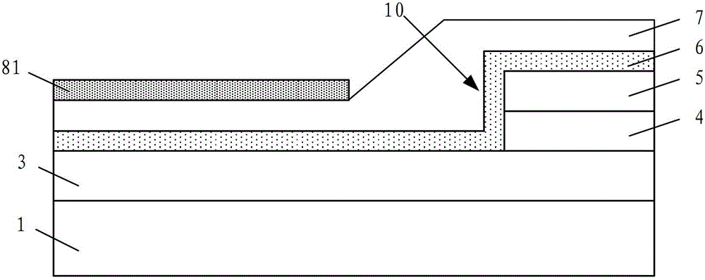
[0126] refer to Figure 4 , the array substrate of the embodiment of the present invention may include:
[0127] Substrate 1;
[0128] A gate electrode and a gate line formed by a gate metal layer on the substrate 1 (not shown in the figure);
[0129] a gate insulating layer 3 located on the substrate 1 formed with the gate electrode and the gate line;
[0130] an active layer 4 located on the gate insulating layer 3;
[0131] A source electrode (not shown in the figure), a drain electrode 5 and a data line (not shown in the figure) located on the active layer 4;
[0132] A pixel electrode 6 with a step portion 10 located on the substrate 1 formed with the source electrode, the drain electrode 5 and the data line, the pixel electrode 6 is connected to the drain electrode 5;
[0133] a passivation layer 7 located on the substrate 1 on which the pixel electrode 6 is formed, a third via hole 13 is formed on the passivation layer 7, and the third via hole 13 straddles the leve...
Embodiment 3
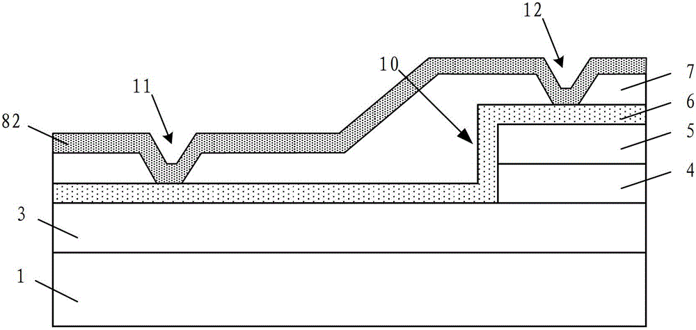
[0138] refer to Figure 5 , the array substrate of the embodiment of the present invention may include:
[0139] Substrate 1;
[0140] A gate electrode (not shown in the figure), a gate line (not shown in the figure) and a second connection part 2 formed by a gate metal layer on the substrate 1, the second connection part 2 is connected to the gate electrode and the gate line disconnected;
[0141] a gate insulating layer 3 located on the substrate 1 on which the gate electrode, gate line and second connecting portion 2 are formed, and a fourth via hole 14 and a fifth via hole 15 are formed on the gate insulating layer 3;
[0142] an active layer 4 located on the gate insulating layer 3;
[0143] A source electrode (not shown in the figure), a drain electrode 5 and a data line (not shown in the figure) located on the active layer 4;
[0144] A pixel electrode 6 with a step portion 10 located on the substrate 1 formed with the source electrode, the drain electrode 5 and the...
PUM
 Abstract
Description
Claims
Application Information