Thin-film transistor, TFT-array substrate, liquid-crystal display device and method of fabricating the same

Active Publication Date: 2007-04-19
NEC LCD TECH CORP
View PDF3 Cites 21 Cited by
  • Summary
  • Abstract
  • Description
  • Claims
  • Application Information

AI Technical Summary

Benefits of technology

[0047] Accordingly, the etching profile in the etching process of the passivation layer and the gate insulating layer c

Problems solved by technology

In this case, however, the raised etch rate of the photoresist mask is unable to follow the raised etch rates of the passivation layer and the gate insulating layer and as a result, there is a possibility that the etching profile of the contact holes penetrating the passivation layer and the gate insulating layer is square or inverted tapered.
If so, a conductive layer to be formed on the passivation layer to contact the underlying gate layer or drain layer will be divided or cut in the contact holes, resulting in point defects or the like of the LCD device.
Accordingly, point defects or the like will occur in the first prior-art LCD device.
Accordingly, the pixel electrode layer 107, which is disposed on the passivatio

Method used


Image

  • Thin-film transistor, TFT-array substrate, liquid-crystal display device and method of fabricating the same
  • Thin-film transistor, TFT-array substrate, liquid-crystal display device and method of fabricating the same
  • Thin-film transistor, TFT-array substrate, liquid-crystal display device and method of fabricating the same

Examples


first embodiment

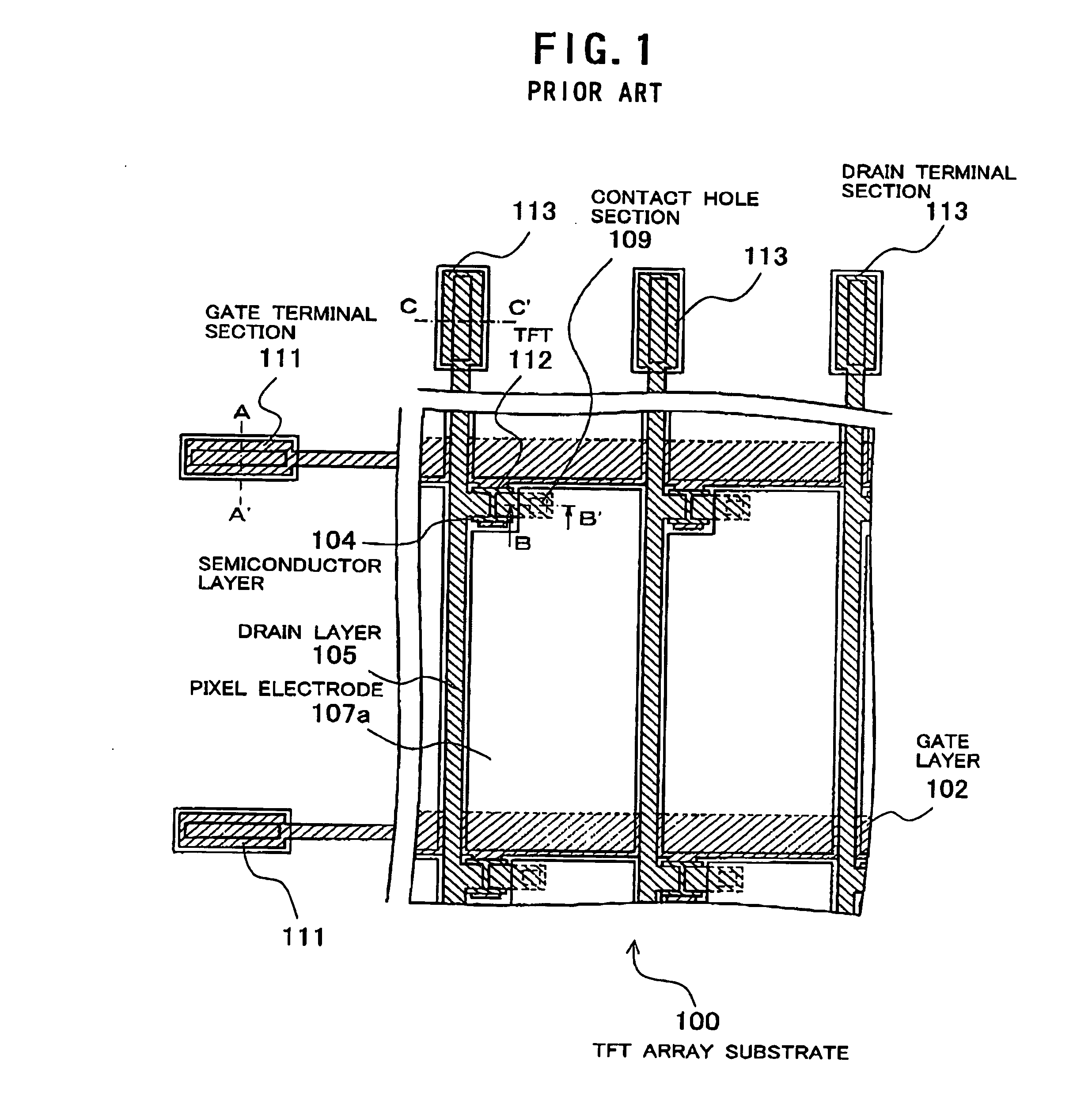
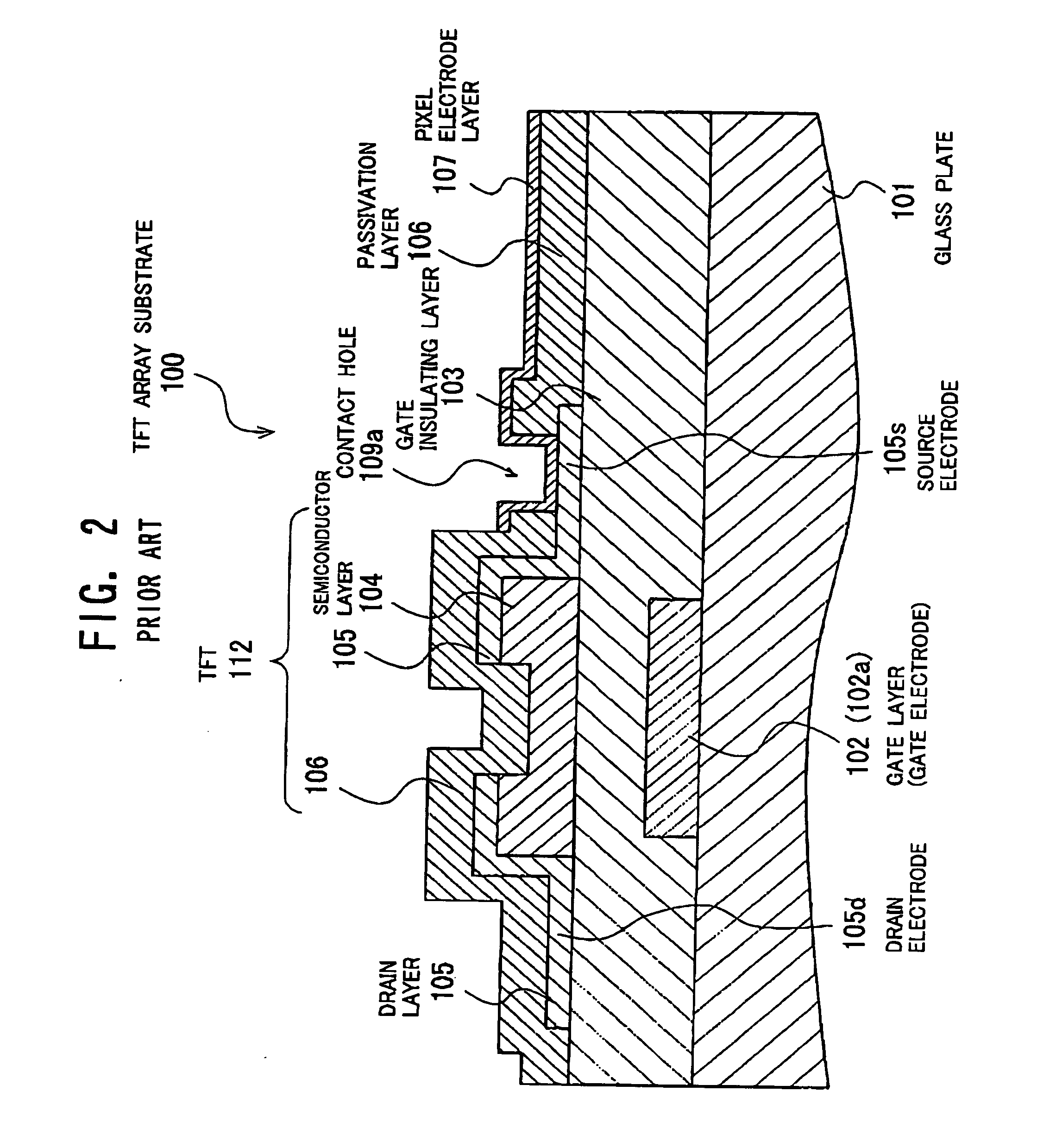
[0108]FIG. 9 schematically shows the structure of a TFT array substrate 10 of a LCD device according to a first embodiment of the present invention. FIG. 13 schematically shows a plan view of the substrate 10 according to the first embodiment, which is substantially the same as that of FIG. 1.

[0109] As shown in FIGS. 9 and 13, a patterned conductive gate layer 2 is formed on a transparent insulating plate 1 (e.g., a glass plate). The gate layer 2 is used to form gate lines, gate electrodes 2a, and gate terminals. On the gate layer 2 (i.e., the gate electrodes 2a), a gate insulating layer 3 is formed to cover the gate electrodes 2a. Island-shaped semiconductor layers 4 are formed on the gate insulating layer 3 to overlap with the corresponding gate electrodes 2a. On the semiconductor layers 4, a patterned conductive drain layer 5 is formed. The drain layer 5 is used to form drain lines, drain electrodes 5d, source electrodes 5s, and drain terminals. On the drain layer 5, a passivati...

second embodiment

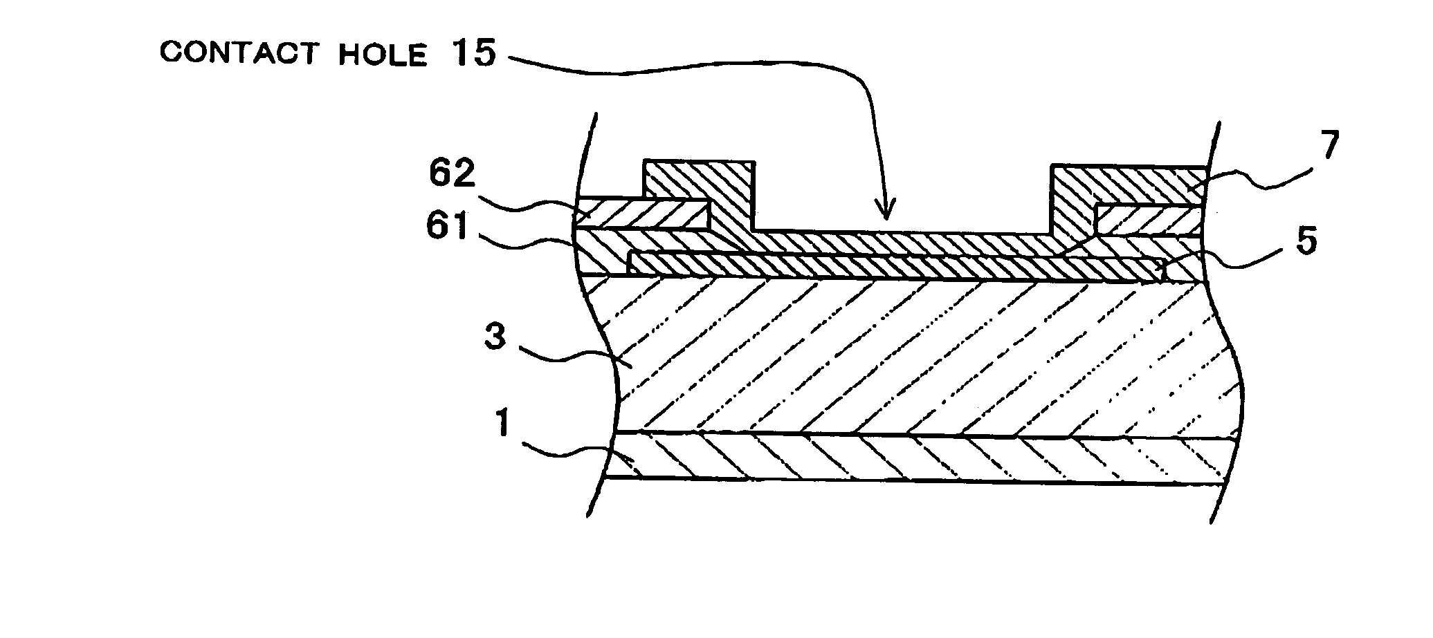
[0137]FIG. 14 schematically shows the structure of a TFT array substrate 10a of a LCD device according to a second embodiment of the present invention. Since the structure of the substrate 10a is the same as that of the substrate 10 of FIGS. 9 and 13 except that a passivation layer 60a has a three-layer structure comprising first, second, and third sublayers 61a, 62a, and 63a. Therefore, explanation about the substrate 10a of the second embodiment is omitted here by attaching the same reference symbols as those in the first embodiment.

[0138] The etch rate of the third sublayer 63a is the highest and the etch rate of the first sublayer 61a is the lowest. The etch rate of the second sublayer 62a is middle. Thus, the etch rates of the sublayers 61a, 62a, and 63a decrease from the top sublayer (i.e., the third sublayer 63a) disposed at the top of the layer 60a to the bottom sublayer (i.e., the first sublayer 61a) disposed at the bottom thereof.

[0139] The etch rate of the next sublayer...


PUM


Abstract

A thin-film transistor includes a gate layer, a gate insulting layer, a semiconductor layer, a drain layer, a passivation layer (each of which being formed on or over an insulating substrate), and a conductive layer formed on the passivation layer. The conductive layer is connected to the gate layer or the drain layer by way of a contact hole penetrating at least the passivation layer. The passivation layer has a multiple-layer structure comprising at least a first sublayer and a second sublayer stacked, the first sublayer having a lower etch rate than that of the second sublayer. The first sublayer is disposed closer to the substrate than the second sublayer. The second sublayer has a thickness equal to or less than that of the conductive layer. The shape or configuration of the passivation layer and the underlying gate insulating layer can be well controlled in the etching process, and the conductive layer formed on the passivation layer is prevented from being divided.

Description

BACKGROUND OF THE INVENTION [0001] 1. Field of the Invention [0002] The present invention relates to a Thin-Film Transistor (TFT) and a method of fabricating the same and more particularly, to a TFT, a TFT array substrate, and a Liquid-Crystal Display (LCD) device, and methods of fabricating them, where the etching profile of an insulating layer is controllable in an etching process. The invention is applicable not only to LCD devices, but also to plasma display devices and display devices employing organic ElectroLuminescence (EL) or the like. [0003] 2. Description of the Related Art [0004] Generally, the LCD device comprises a TFT substrate on which TFTs are arranged in a matrix array, an opposite substrate, and a liquid crystal layer sandwiched by the TFT substrate and the opposite substrate. Pixels are defined on the TFT array substrates. The TFTS, which are arranged to correspond to the respective pixels, turn the optical paths on or off in the respective pixels, thereby displa...

Claims


Application Information

Patent Timeline
IPC IPC(8): H01L21/84H01L21/00H01L29/04H01L29/10H01L29/15H01L31/00H01L31/036
CPCG02F1/136227H01L27/1248H01L27/12H01L21/76804G02F1/136
Inventor TANAKA, HIROAKI
Owner NEC LCD TECH CORP
Why Eureka
Try Eureka