Check patentability & draft patents in minutes with Patsnap Eureka AI!

Array substrate

An array substrate and substrate technology, applied in nonlinear optics, instruments, optics, etc., can solve problems such as disconnection of data lines 10, lower yield rate of liquid crystal panels, and failure of normal alignment of liquid crystal molecules, so as to reduce scrap rate and improve uniformity sexual effect

Active Publication Date: 2012-10-31
SHENZHEN CHINA STAR OPTOELECTRONICS TECH CO LTD
View PDF7 Cites 2 Cited by
  • Summary
  • Abstract
  • Description
  • Claims
  • Application Information

AI Technical Summary

Problems solved by technology

However, in the process of forming the data line 10, due to the influence of various factors, the data line 10 is often disconnected.
As shown in the figure, if the point D in the data line 10 is disconnected, when the electrical signal is input from the signal input module 20 to the data line 10 via the transmission line 30, the electrical signal reaches the point D through the first end 10a, because the point D There is an open circuit, and the electrical signal cannot be transmitted through the point D, so the part of the data line 10 except the first end 10a to the point D has no electrical signal, so the corresponding liquid crystal molecules cannot be aligned normally, resulting in display defects of the liquid crystal panel. And reduce the yield of LCD panel

Method used


Image

  • Array substrate
  • Array substrate
  • Array substrate

Examples


Embodiment Construction

[0026] It should be understood that the specific embodiments described here are only used to explain the present invention, not to limit the present invention.

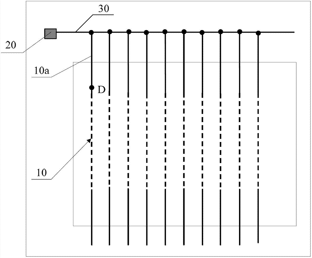
[0027] refer to figure 2 , figure 2 It is a schematic structural diagram of the first embodiment of the array substrate of the present invention. The array substrate provided in this embodiment includes a substrate 40, several data lines 10 arranged in parallel on the substrate 40, a signal input module 20 for inputting an alignment electrical signal, and at least one transmission line 30; the data line has a first end 10a and the second end 10b, one end of the transmission line 30 is connected to the signal input module 20, and connected to the first end 10a and the second end 10b of the data line 10 respectively. After the alignment electrical signal passes through the signal input module 20 and the transmission line 30 , it is input into the data line 10 from the first end 10 a and the second end 10 b of the da...


PUM


Abstract

The invention discloses an array substrate. The array substrate comprises a substrate, a plurality of data lines which are arrayed on the substrate in parallel, a signal input module for inputting a power distribution signal, and at least one transmission line, wherein each data line is provided with a first end and a second end; and one end of the transmission line is connected with the signal input module and is respectively connected with the first end and the second end of each data line. The power distribution signal passes through the first ends and the second ends of the data lines from the transmission line to be input into the data lines, so that when the data lines are powered off, the power distribution signal can be normally input into the parts at the two sides of broken points of the data lines; and therefore, the consistency of liquid crystal molecule directions is improved and the rejection rate of a liquid crystal panel is reduced.

Description

technical field [0001] The invention relates to the field of liquid crystal display, in particular to an alignment circuit of an array substrate. Background technique [0002] With the development of electronic technology, flat panel display devices have been rapidly developed, such as liquid crystal display devices, plasma display devices and OLED (Organic Light-Emitting Diode, organic light-emitting diode) display devices. Among flat panel display devices, liquid crystal display devices are gradually replacing cold cathode display devices due to their advantages of low weight, small size, and low energy consumption. PSVA (Polymer Stabilize Vertical Alignment, polymer stabilized vertical alignment mode) is widely used in liquid crystal displays. [0003] In the PSVA display mode, reactive monomers are added to the negative liquid crystal. After the liquid crystal cell is formed, a voltage is applied across the liquid crystal cell. Under the excitation of ultraviolet light,...

Claims


Application Information

Patent Timeline
IPC IPC(8): G02F1/1362G02F1/133
CPCG02F1/1337G02F1/133G02F1/133788G02F1/13775
Inventor 徐亮
Owner SHENZHEN CHINA STAR OPTOELECTRONICS TECH CO LTD
Features
  • R&D
  • Intellectual Property
  • Life Sciences
  • Materials
  • Tech Scout
  • Unparalleled Data Quality
  • Higher Quality Content
  • 60% Fewer Hallucinations
Learn More