Method for post-processing blind hole of circuit board

A processing method and circuit board technology, applied in the direction of forming the electrical connection of printed components, etc., can solve the problems of insufficient electroplating and deep plating capacity, increase production cost, long processing time, etc., to save production time, production cost, and reduce processing difficulty. Effect

Inactive Publication Date: 2012-10-31
SHENZHEN SUNTAK MULTILAYER PCB
View PDF2 Cites 10 Cited by
  • Summary
  • Abstract
  • Description
  • Claims
  • Application Information

AI Technical Summary

Problems solved by technology

Using the electroplating hole filling process to process the blind holes of the circuit board requires the use of special electroplating additives. This electroplating additive will be much more expensive than ordinary electroplating additives, which will greatly increase the production cost of the enterprise.
In addition, the inorganic components in the hole-filling electroplating potion are of the "high copper and low acid" type, that is, the concentration of copper sulfate is relatively high and the concentration of sulfuric acid is relatively low. Copper low-acid" type electroplating solution, the deep plating ability of electroplating is not enough, which will easily increase the difficulty of etching in the subsequent process
[0004] In addition, the process of hole filling and electroplating is prone to defects such as hole filling and insufficient filling, and the processing time is long, which wastes a lot of manpower and material resources, which is not conducive to creating benefits

Method used


Image

  • Method for post-processing blind hole of circuit board
  • Method for post-processing blind hole of circuit board
  • Method for post-processing blind hole of circuit board

Examples


Embodiment Construction

[0023] In order to fully understand the technical content of the present invention, the technical solutions of the present invention will be further introduced and illustrated below in conjunction with specific examples, but not limited thereto.

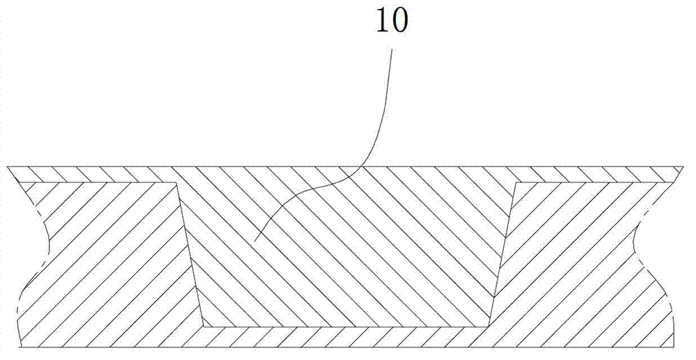
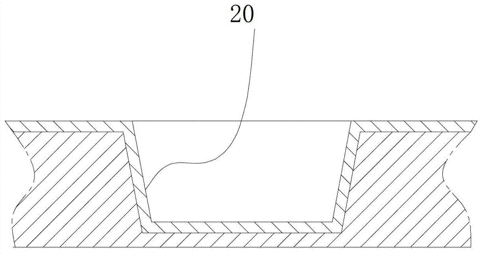
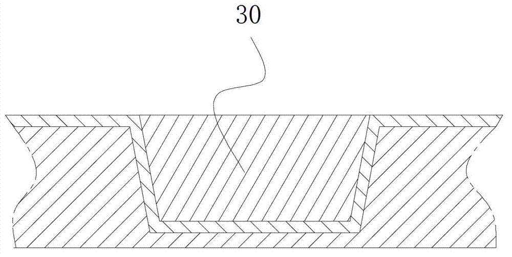
[0024] Such as Figure 2 to Figure 4 As shown, a post-processing method of a circuit board blind hole of the present invention, the method is a post-processing for the blind hole of a circuit board, comprising the following steps:

[0025] First, copper-plate the inner wall of the blind hole of the circuit board, and the thickness of the copper plating is 20-25um, such as figure 2 shown;

[0026] Secondly, vacuum plug the copper-plated blind hole, and grind the filling surface of the blind hole, such as image 3 shown;

[0027] Finally, copper plating is carried out on the surface of the filled blind hole after grinding, and the thickness of the copper plating on the surface is 10-15um, such as Figure 4 shown;

[0028] Wherein...


PUM

PropertyMeasurementUnit
dielectric lossaaaaaaaaaa

Abstract

The invention discloses a method for post-processing a blind hole of a circuit board. The method comprises the following steps of: firstly, carrying out inner-wall copper plating on the blind hole of an HDI (High Density Interconnect) board; secondly, carrying out vacuum hole filling on the copper-plated blind hole; then, grinding and flattening a filling surface of the blind hole; and finally, carrying out surface copper plating on the filling surface, which is ground and flattened, of the blind hole. The vacuum hole filling is achieved by filling fluid-like resin in the blind hole in a vacuum manner. According to the method, the low-cost resin is adopted to carry out filling treatment on the blind hole by using a vacuum manner; and compared with the existing copper-sinking filling manner (via filling plating process), the method has the advantages that the production cost is saved, the difficulty of processing is reduced, the rejection rate is reduced, and the production time is saved.

Description

technical field [0001] The invention relates to a method for manufacturing a circuit board, more specifically a method for manufacturing a blind hole of a circuit board. Background technique [0002] The size of electronic products is becoming thinner and smaller, and stacking vias directly on vias and blind vias (Via on Hole or Via on Via) is a design method for high-density interconnection. To do a good job of stacking holes, the flatness of the bottom of the hole should be done first. There are several methods for typical flat hole surfaces, and the Via Filling Plating process is one of the representative ones. At present, for the post-processing of blind holes, the electroplating hole filling process is mostly used (such as figure 1 As shown) to treat the blind hole, that is, through the action of special electroplating additives (brightener, leveling agent, wetting agent), the blind hole is filled and leveled during the electroplating process, so as to achieve the fun...

Claims


Application Information

Patent Timeline
Patent Type & Authority Applications(China)
IPC IPC(8): H05K3/42
Inventor 邓丹刘东叶应才张岩生宋建远
Owner SHENZHEN SUNTAK MULTILAYER PCB
Why Eureka
Try Eureka