Method for manufacturing p-type and n-type semiconductor light extraction vertical conduction LED (light-emitting diode)

A technology of light-emitting diodes and semiconductors, which is applied to semiconductor devices, electrical components, circuits, etc., can solve the problems of difficulty in punching sapphire substrates, failure of electrodes to obtain optimal light output, and huge impact on yield, so as to increase the amount of light output. and luminous efficiency, improve yield, and ensure the effect of efficiency

Active Publication Date: 2015-02-25
NANTONG YAOLONG METAL MFG CO LTD
View PDF6 Cites 0 Cited by
  • Summary
  • Abstract
  • Description
  • Claims
  • Application Information

AI Technical Summary

Problems solved by technology

Although the heat dissipation characteristics of new substrate materials are generally superior to those of sapphire substrates, the process of attaching and removing sapphire has a huge impact on yield
Substrate drilling is a better option. The non-light-emitting surface is bonded with heat-dissipating metal, which is very helpful for the heat dissipation of LEDs, but it is not easy to drill holes in the sapphire substrate, and after drilling, the electrode design relationship between the light-emitting surface and the reflective surface emits light. efficiency
The existing technology uses a sapphire substrate to drill holes, but the design of the electrode fails to obtain the best light output

Method used


Image

  • Method for manufacturing p-type and n-type semiconductor light extraction vertical conduction LED (light-emitting diode)
  • Method for manufacturing p-type and n-type semiconductor light extraction vertical conduction LED (light-emitting diode)
  • Method for manufacturing p-type and n-type semiconductor light extraction vertical conduction LED (light-emitting diode)

Examples


Embodiment 1

[0048] Example 1: p-type semiconductor emits light

[0049] The manufacturing method of the p-type semiconductor light-emitting vertical conduction light-emitting diode:

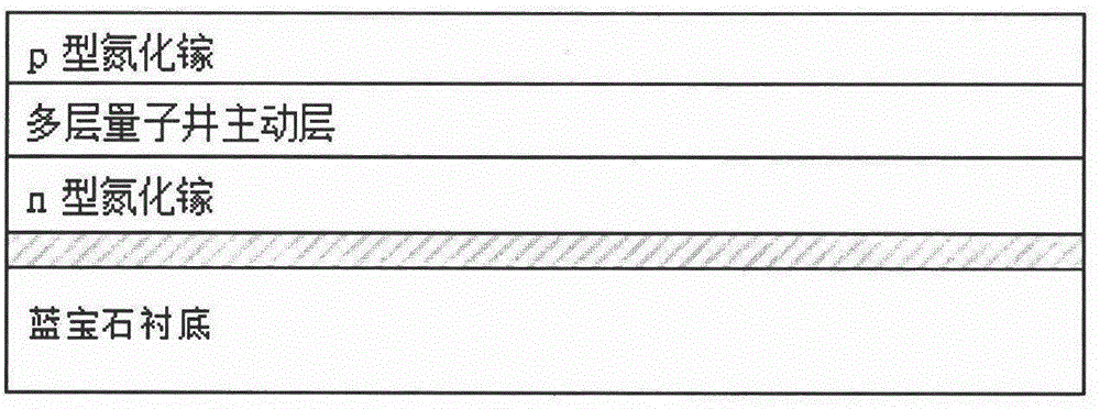
[0050] (1) if figure 1As shown, a sapphire substrate is provided, and a light-emitting structure of a light-emitting diode is epitaxially grown on the front surface of the substrate. The light-emitting structure includes a GaN buffer layer and a GaN light-emitting diode epitaxial layer formed in sequence. The GaN light-emitting diode epitaxial layer includes an n-type GaN layer, a multi-layer quantum well active layer (multi-quantum well active layer, MQW active layer, that is, a light-emitting layer) and a p-type nitride layer arranged in sequence. Gallium layer;

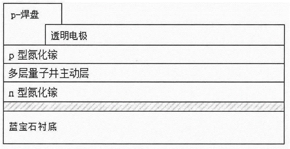
[0051] (2) if figure 2 As shown, a p-electrode structure is formed on the p-type gallium nitride layer. The p-electrode structure includes a transparent electrode and a p-bonding pad arranged in sequence, and can be connected to an external c...

Embodiment 2

[0071] Example 2: n-type semiconductor light output

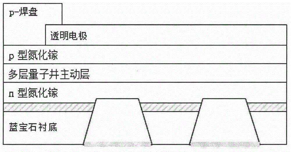
[0072] Such as Figure 12 As shown, the difference between this embodiment and Embodiment 1 is that the structure of the p-electrode in this embodiment is exactly the structure of the n-electrode in Embodiment 1, and the structure of the n-electrode in this embodiment is exactly the structure of the n-electrode in Embodiment 1. In the structure of the p-electrode, the pad in this embodiment is not a p-pad, but an n-pad. Figure 13 yes Figure 12The bottom view of , showing the light-emitting surface (reverse surface, n-electrode side) of the n-type semiconductor light-emitting vertical conduction light-emitting diode. Figure 14 yes Figure 12 The top view of , shows the front side (p-electrode side) of the n-type semiconductor light-emitting vertical conduction light-emitting diode, and the dotted line is the pattern of the n-pad and the sapphire hole on the back side.


PUM

PropertyMeasurementUnit
wavelengthaaaaaaaaaa
thicknessaaaaaaaaaa

Abstract

Disclosed is a method for manufacturing a p-type semiconductor light-output vertical conduction light-emitting diode (LED). The method comprises the following steps: providing a substrate, epitaxially growing a luminous structure of the LED on the front side of the substrate, the luminous structure comprising a gallium nitride buffer layer and a gallium nitride LED epitaxial layer which are sequentially formed, and the gallium nitride LED epitaxial layer comprising an n-type gallium nitride layer, a luminous layer and a p-type gallium nitride layer which are sequentially arranged; forming a p-electrode structure on the p-type gallium nitride layer, the p-electrode structure comprising a transparent electrode and a p-pad which are sequentially arranged; forming a hole on the back side of the substrate, and remaining on the n-type gallium nitride layer; and forming an n-electrode structure on the back side of the substrate, the n-electrode structure comprising a transparent electrode, a reflecting metal layer and a joint metal layer which are sequentially arranged. Also disclosed is a method for manufacturing an n-type semiconductor light-output vertical conduction LED. By means of the present invention, the light-output amount and the luminous efficiency of the vertical conduction nitride LED can be improved.

Description

technical field [0001] The invention relates to the field of manufacturing light-emitting diodes, in particular to a manufacturing method of p-type and n-type semiconductor light emitting vertical conduction light-emitting diodes. Background technique [0002] The advantages of vertical conduction light-emitting diodes: 1. The current path is short, so the forward voltage is small; 2. The current distribution is uniform, reducing the phenomenon of current crowding; 3. The number of bonding wires can be reduced; 4. The non-light-emitting surface can be bonded for heat dissipation layer to reduce light decay. [0003] Because the substrate commonly used for nitride light-emitting diodes is sapphire material (Al 2 o 3 ), which is an insulator, and to achieve vertical conduction, the sapphire substrate must be removed, or a hole must be drilled in the sapphire substrate. Because the sapphire substrate supports the semiconductor device, before removing the sapphire substrate, ...

Claims


Application Information

Patent Timeline
Patent Type & Authority Patents(China)
IPC IPC(8): H01L33/00
CPCH01L33/20H01L33/42H01L33/382H01L33/405
Inventor 廖丰标顾玲
Owner NANTONG YAOLONG METAL MFG CO LTD
Why Eureka
Try Eureka