Device and method used for measuring film thickness

A technology for measuring devices and film thickness, applied in measuring devices, optical devices, instruments, etc., can solve the problems of narrow spectral width, low resolution, low precision, etc., and achieve expanded spectrum range, improved resolution, and high-precision film thickness measured effect

Inactive Publication Date: 2012-11-14
BEIJING BOE OPTOELECTRONCIS TECH CO LTD
View PDF8 Cites 15 Cited by
  • Summary
  • Abstract
  • Description
  • Claims
  • Application Information

AI Technical Summary

Problems solved by technology

[0011] To sum up, the existing film thickness measurement devices, such as the first device, can only obtain the light intensity of certain wavelengths by light separation due to the grating used in its own light-splitting unit, and the spectral width of the fitting sampling point is relatively narrow. Then cause the problem of lower resolution; and for the second device, because it uses optical filters to obtain light intensities of different wavelengths, and due to the determination of the number of collection holes on the filter and the film attached to the collection holes The determination of transmitted light makes the number and position of light intensity sampling points fixed, and the accuracy is relatively low

Method used


Image

  • Device and method used for measuring film thickness
  • Device and method used for measuring film thickness
  • Device and method used for measuring film thickness

Examples


Embodiment Construction

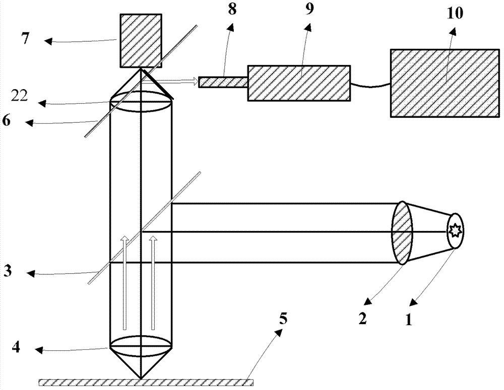
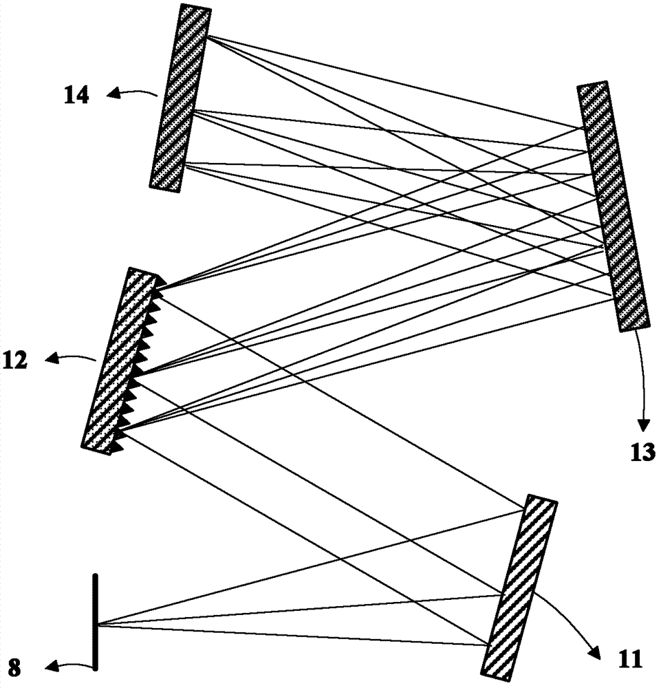
[0046] Since a prism can split a beam of light in a continuous spectrum, in some measurement systems that require high resolution, a prism can be used as a spectroscopic device to improve resolution.
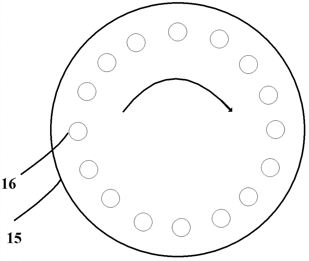
[0047] The basic idea of ​​the present invention is: a kind of film thickness measuring device, comprises collimating lens, first half-mirror, objective lens, second half-mirror, collecting optical fiber, computer and spectroscopic unit; Wherein, said spectroscopic The unit is used to perform spectroscopic processing on the light collected by the collection fiber, and separate and obtain light of each wavelength; the computer is used to obtain the intensity of light of different wavelengths, and calculate the film thickness of the measured object.

[0048] In order to make the object, technical solution and advantages of the present invention clearer, the present invention will be further described in detail by citing the following embodiments and referring to the accompanying dr...


PUM


Abstract

The invention provides a device and a method used for measuring film thickness. The device comprises a collimating lens, a first half-transmitting half-reflecting mirror, a field lens, a second half-transmitting half-reflecting mirror, a collection optical fibre, a picture sensor, a computer and a beam split unit, wherein the beam split unit is used for carrying out beam split treatment on the light collected by the collection optical fibre so as to obtain light of each wavelength in a separate manner; and the computer is used for obtaining the intensity of the light with different wavelengths so as to obtain the film thickness of an analyte through calculating. The device provided by the invention has the advantages that the beam split unit is used for carrying out beam split treatment on the light collected by the collection optical fibre so as to obtain the light of each wavelength in the separate manner, the spectral range of a sample point of the device used for measuring film thickness is enlarged, and the distinguishability is improved; and furthermore, the quantity and position of the sample points can be controlled in a flexible manner through the position adjustment of an optical fibre probe, so that the flexibility of processing data is improved and the high-precision film thickness measurement is realized.

Description

technical field [0001] The invention relates to the field of film thickness measurement, in particular to a film thickness measurement device and method. Background technique [0002] In the production process of Thin Film Transistor-Liquid Crystal Display (TFT-LCD), it is often necessary to measure semiconductor thin films. The basic structure of the existing film thickness measurement device is as follows: figure 1 As shown, the light source 1 emits a beam of light, which forms a parallel beam through the collimator lens 2, reaches the first half-mirror 3, half of the light reaches the objective lens 4 after reflection, and shines on the sample 5, and the light reflected by the sample 5 passes through the mirror. The cylinder reaches the eyepiece 22, and part of the transmitted light by the second half-mirror 6 at the eyepiece 22 reaches the imaging charge-coupled device (Charge-Coupled Device, CCD) 7 to obtain the image information of the sample 5, while the other part of...

Claims


Application Information

Patent Timeline
Patent Type & Authority Applications(China)
IPC IPC(8): G01B11/06
CPCG01B11/0625
Inventor 曲连杰郭建王德帅朱朋举
Owner BEIJING BOE OPTOELECTRONCIS TECH CO LTD
Why Eureka
Try Eureka