Manufacture method of semiconductor device

A semiconductor and device technology, applied in the field of semiconductor device manufacturing, can solve problems such as difficult alignment, and achieve the effect of avoiding alignment problems

Active Publication Date: 2012-11-14
SEMICON MFG INT (SHANGHAI) CORP
View PDF5 Cites 10 Cited by
  • Summary
  • Abstract
  • Description
  • Claims
  • Application Information

AI Technical Summary

Problems solved by technology

[0014] However, the mask patterns used in these three times have the problem of difficulty in alignment.

Method used


Image

  • Manufacture method of semiconductor device
  • Manufacture method of semiconductor device
  • Manufacture method of semiconductor device

Examples


Embodiment Construction

[0045] A method of manufacturing a semiconductor device according to the present invention will be described below with reference to the accompanying drawings.

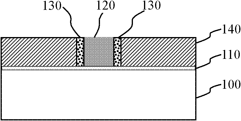
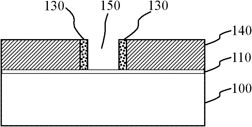
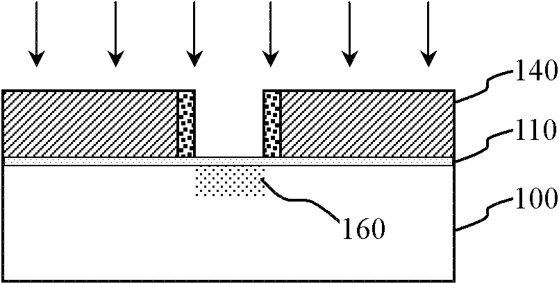
[0046] At present, the manufacturing process of transistors with HKMG (high dielectric constant insulating layer + metal gate) structure is divided into the gate-first process school represented by IBM and the gate-last process school represented by Intel.

[0047] In the gate-last process, after removing the dummy gate, an opening corresponding to the channel region is naturally formed. The inventors of the present invention thus creatively propose that, by means of the opening for implanting germanium, there is no need to additionally provide a mask corresponding to the channel region for germanium implantation. Since the use of a mask corresponding to the channel region is reduced, a problem that a plurality of mask patterns need to be aligned can be avoided.

[0048] Refer below Figures 1A-1E with Figures 2A-...


PUM


Abstract

The invention relates to a manufacture method of a semiconductor device. The method comprises the following steps that a forged grid electrode and an insulation material layer are formed on a substrate, the forged grid electrode is embedded in the insulation material layer, the forged grid electrode is removed so that an opening is formed in the insulation material layer, the insulation material layer is used as a mask, and carbon ions or germanium ions are injected into the substrate through the opening. According to the method, the alignment problem caused by the use of the mask corresponding to a ditch for many times is solved.

Description

technical field [0001] The invention relates to semiconductor technology, in particular to a method for manufacturing a semiconductor device. Background technique [0002] With the continuous development of semiconductor technology, the feature size of MOSFET has been continuously reduced, and the problem of reduced carrier mobility has attracted great attention in the industry, and several solutions to enhance carrier mobility have been proposed. [0003] Some of these schemes achieve the purpose of enhancing carrier mobility by applying stress in the channel region of the MOSFET. [0004] If stress is applied to the channel region of a MOS device, causing it to strain, its carrier mobility can be affected. Specifically, NMOS devices are electronically conductive, so the larger the lattice spacing, the smaller the effect of lattice scattering, the greater the electron mobility, and the greater the drive current, so it is desirable to apply tensile stress to the channel suc...

Claims


Application Information

Patent Timeline
Patent Type & Authority Applications(China)
IPC IPC(8): H01L21/336H01L21/266
CPCH01L29/66545H01L29/66477H01L21/26506H01L29/66537H01L29/7849H01L29/1054
Inventor 三重野文健
Owner SEMICON MFG INT (SHANGHAI) CORP
Why Eureka
Try Eureka