Manufacturing method of patch type LED (Light-Emitting Diode) module

A technology of LED modules and manufacturing methods, which is applied in the directions of printed circuit manufacturing, final product manufacturing, sustainable manufacturing/processing, etc., and can solve the problem of multi-material cost, long process time, and low reliability of single LED light source processing Process and other issues, to achieve the effect of low chip failure rate, short process time, saving packaging materials and packaging process time

Inactive Publication Date: 2012-11-14
XIAMEN G WATT LIGHTING TECHNOLOGY INC
View PDF8 Cites 13 Cited by
  • Summary
  • Abstract
  • Description
  • Claims
  • Application Information

AI Technical Summary

Problems solved by technology

[0006] The main purpose of the present invention is to provide a method for manufacturing a chip-type LED module, which solves the problem of excessive material cost due to the large-scale production of LED modules; The

Method used


Image

  • Manufacturing method of patch type LED (Light-Emitting Diode) module
  • Manufacturing method of patch type LED (Light-Emitting Diode) module
  • Manufacturing method of patch type LED (Light-Emitting Diode) module

Examples


Embodiment 1

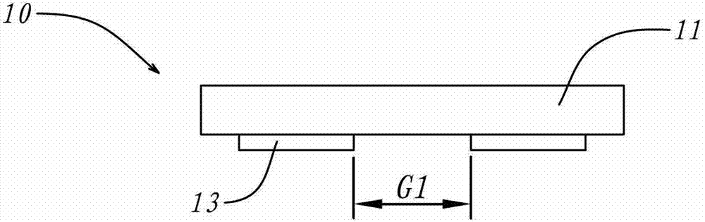
[0047] figure 1 As shown, the flip-chip structure of the LED chip 10 used in the present invention, the main body 10 is a part of semiconductor material, below are positive and negative metal electrodes that form ohmic contact with the main body 10, on the plane below the main body 10 Inside, the distance G1 between the metal electrodes 13 is 80 μm; the light-emitting surface 12 and the metal electrode 13 of the conductive part are located on the two sides of the main body 10 for this type of flip-chip structure LED chip, which does not interfere with each other, and its luminous efficiency is high.

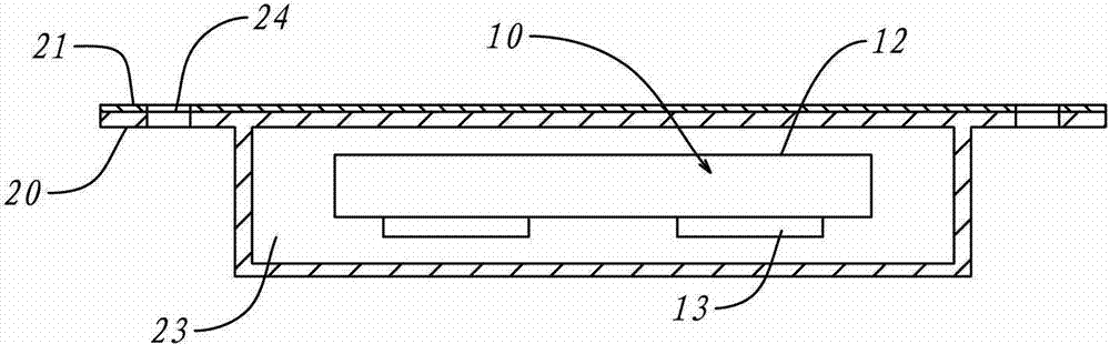
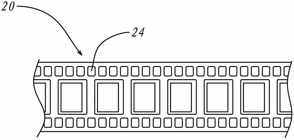
[0048] Such as figure 2 with image 3 As shown, the LED chips 10 are put into the braid 20 one by one, and each LED chip occupies an accommodating space 23 independent of each other; and the metal electrode 13 of the LED chip 10 is located at the bottom of the accommodating space 23; the light-emitting surface 12 is located at the accommodating space 23 The opening of the space. Wh...

Embodiment 2

[0060] Such as Picture 9 , Picture 10 , The two state diagrams of the second embodiment of the present invention:

[0061] Compared with the first embodiment, the difference between this embodiment and the first embodiment is that during the mounting step, the substrate 40 has an auxiliary colloid 45 between the pads 41. The auxiliary colloid 45 is used for when the LED chip 10 is large in volume. It is difficult to temporarily fix the LED chip 10 on the substrate due to the tension of the solder paste 42. The auxiliary glue 45 serves as a temporary component to make the LED chip 10 and the pad 41 relatively accurate and stable, and there will be no posture deviation even after passing through the reflow oven. .

[0062] The other difference is that after the fixing step of the LED chip 10 is completed, the light-emitting surface of the LED chip 10 is covered with a fluorescent film 50. This fluorescent film is in the form of a whole film and is formed separately, so it can be d...


PUM

PropertyMeasurementUnit
Wavelengthaaaaaaaaaa

Abstract

The invention discloses a manufacturing method of a patch type LED (Light-Emitting Diode) module. The manufacturing method is characterized by comprising the following steps of: preparing materials; providing LED chips with flip chip structures, wherein one face of each LED chip is provided with a metal electrode, and the surface intervals of the metal electrodes are not smaller than 80 mum; arranging: putting the plurality of chips into a braid, wherein the metal electrodes of the LED chips are positioned at the bottom of a braid accommodating space, and the light emitting surfaces of the LED chips are positioned on the opening of the accommodating space; patching: sucking the LED chips out of the braid by using a vacuum suction nozzle, and placing onto a bonding pad of a substrate, wherein the metal electrodes are opposite to the bonding pad, and the light emitting surfaces of the LED chips face upwards; and fixing: correspondingly fixing and communicating the bonding pad and the metal electrodes. A braid loading way is directly adopted for flip chip LED chips, so that encapsulation of a single LED light source is avoided, and the encapsulating materials, encapsulating process time and production line of a single LED light source are saved.

Description

Technical field [0001] The invention relates to a production method for manufacturing a patch type LED module. Background technique [0002] With the development of lighting LED technology, compared with traditional incandescent lamps and halogen lamps, LEDs have obvious advantages in energy saving, reliability, and longevity, and can gradually achieve the lighting performance of fluorescent lamps, such as light efficiency and display. In terms of color index and life span. Therefore, worldwide, the development of lighting LEDs is in the ascendant, and the annual output of LED light sources is gradually increasing. [0003] Compared with traditional light sources, LED light sources have some obvious characteristics. Usually, in terms of volume, LED light sources are based on a single chip, with electrodes, phosphors, packaging structures, etc., which have a smaller volume and With less luminous flux, if it is necessary to form a suitable lighting fixture, it is inevitable to use ...

Claims


Application Information

Patent Timeline
IPC IPC(8): H01L33/48H01L25/075
CPCH05K2201/10106H05K3/3436H01L33/62H01L2224/16H05K13/0417H05K2203/1366H01L33/486H01L33/00H05K3/3431H05K3/281H05K2203/082H05K2203/048H01L2933/0066Y02P70/50
Inventor 廖泳吕宗宜
Owner XIAMEN G WATT LIGHTING TECHNOLOGY INC
Why Eureka
Try Eureka