
Novel semiconductor lead processing device

A processing device and semiconductor technology, applied in semiconductor/solid-state device manufacturing, electrical components, circuits, etc., can solve problems such as low production efficiency, burrs in the incision, unstable product length, etc., and achieve high production efficiency, no burrs, and products The effect of length stability

Inactive Publication Date: 2012-11-28
HAIAN COUNTY BUSINESS SCHOOL
View PDF0 Cites 0 Cited by
  • Summary
  • Abstract
  • Description
  • Claims
  • Application Information

AI Technical Summary

Problems solved by technology

[0002] Semiconductor wire is a kind of wire with multiple specifications, sizes and shapes dedicated to semiconductors, which is formed by physically changing oxygen-free copper materials into wires with a wire diameter of 1.5mm-4mm, and then stamping and forming. The length of the product produced by the wire processing equipment is unstable, the cut has burrs, and the production efficiency is low

Method used


Image

  • Novel semiconductor lead processing device

Examples


Embodiment Construction

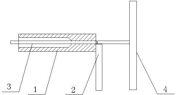
[0009] refer to figure 1 , the specific embodiment adopts the following technical scheme: it includes a threading block 1, a cutter 2, a threading hole 3 and a positioning device 4, a threading hole 3 is arranged in the threading block 1, and the cutter 2 is vertically fixed on the outlet side of the threading hole 3 , The side of the cutter 2 is provided with a positioning device 4 .

[0010] The cutter 2 is closely attached to the outlet of the threading hole 3 .

[0011] When this specific embodiment is used, the wire is passed through the threading hole 3 in the threading block 1 , and when one end of the wire reaches the positioning device 4 , the wire is cut off by the cutter 2 .

[0012] The specific implementation mode can make the product length stable, the incision is flush, no burrs, and the production efficiency is high.


PUM


Abstract

The invention discloses a novel semiconductor lead processing device, and relates to semiconductor processing equipment. The device comprises a threading block (1), a cutter (2), a threading hole (3) and a positioning device (4), wherein the threading hole (3) is arranged in the threading block (1); the cutter (2) is vertically fixed on the exit side of the threading hole (3); and the positioning device (4) is arranged beside the cutter (2). The device disclosed by the invention can realize stable length and flush cut of the product, prevents rough edges, and has high production efficiency.

Description

technical field [0001] The invention relates to a semiconductor processing equipment, in particular to a novel semiconductor processing device. Background technique [0002] Semiconductor wire is a kind of wire with multiple specifications, sizes and shapes dedicated to semiconductors, which is formed by physically changing oxygen-free copper materials into wires with a wire diameter of 1.5mm-4mm, and then stamping and forming. The length of the product produced by the wire processing equipment is unstable, the cut has burrs, and the production efficiency is low. Contents of the invention [0003] The object of the present invention is to provide a novel semiconductor processing device, which can make the length of the product stable, the cuts flush, no burr, and the production efficiency is high. [0004] In order to solve the existing problems of the background technology, the present invention adopts the following technical solutions: it comprises a threading block 1, ...

Claims


Application Information

Patent Timeline
Patent Type & Authority Applications(China)
IPC IPC(8): H01L21/48H01L21/00
Inventor 马东宇
Owner HAIAN COUNTY BUSINESS SCHOOL
Learn More