Supercharge Your Innovation With Domain-Expert AI Agents!

Method for dispensing solder on a substrate and method for mounting semiconductor chips

A semiconductor and substrate technology, applied in semiconductor devices, semiconductor/solid-state device manufacturing, auxiliary devices, etc., can solve problems such as insufficient wetting of substrates, lack of pre-cleaning, etc.

Active Publication Date: 2012-11-28
ESEC
View PDF12 Cites 2 Cited by
  • Summary
  • Abstract
  • Description
  • Claims
  • Application Information

AI Technical Summary

Problems solved by technology

The disadvantage in this method is that the substrate can only be wetted insufficiently without pre-cleaning

Method used


Image

  • Method for dispensing solder on a substrate and method for mounting semiconductor chips
  • Method for dispensing solder on a substrate and method for mounting semiconductor chips
  • Method for dispensing solder on a substrate and method for mounting semiconductor chips

Examples


Embodiment Construction

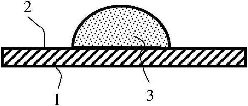
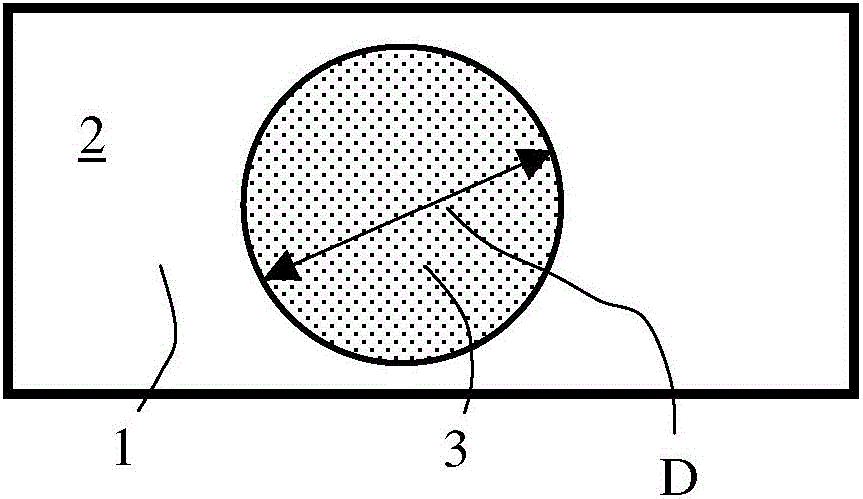
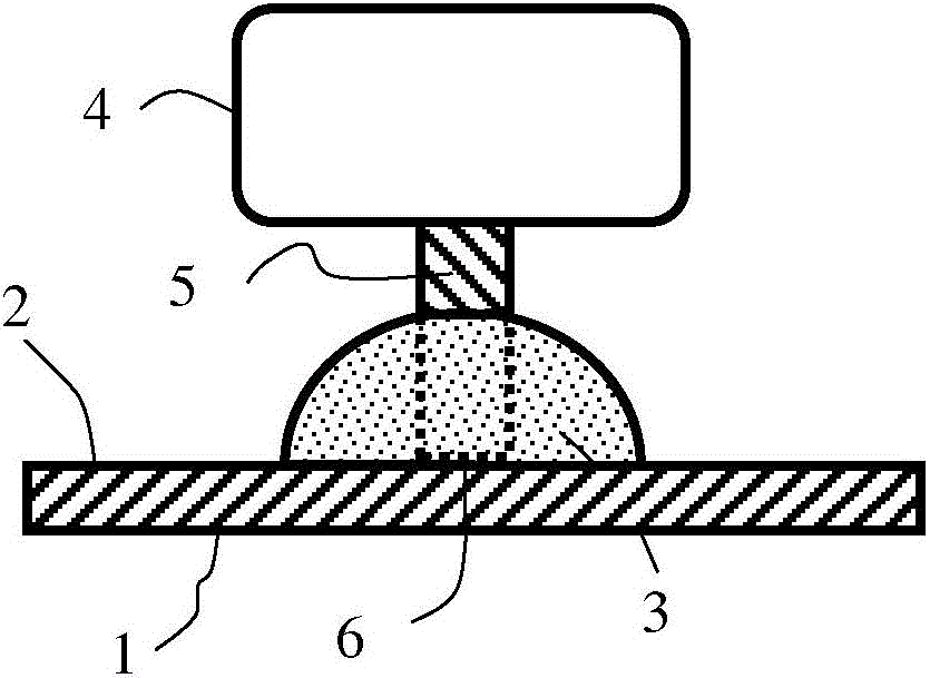
[0025] In practice, semiconductor chips are soldered to substrates with edge dimensions ranging from the submillimeter to the centimeter range. Therefore, the method according to the invention is carried out in a manner which is most suitable for the size of the semiconductor chip and the connection quality required by the application. The mounting of the semiconductor chips takes place by means of automatic assembly machines known as soft solder die bonding machines. The substrate is supplied in a periodic manner to a dispensing station, where solder is applied to the substrate, and then to a bonding station, where a semiconductor chip is placed on the solder portion. For both processes, the substrate is maintained at a temperature above the melting temperature of the solder and typically in an inert gas environment.

[0026] 1 to 4 show a method according to the invention for applying solder to a substrate 1 , based on the example of subsequently placing a medium-sized or l...


PUM


Abstract

The invention relates to a method for dispensing solder and a method for mounting a semiconductor chip on the dispensed solder. The substrate is heated to a temperature which lies above the melting temperature of the solder and a solder portion is applied. A pin is thereafter immersed in the solder portion until it touches the solder portion and presses against the substrate. The pin is subjected to ultrasonic sound in such a way that ultrasonic waves are generated in the pin, which are directed perpendicularly or angularly in relation to the surface of the substrate, and is then moved along a predetermined path in order to distribute the solder. The treatment with ultrasonic sound locally improves the wettability of the substrate. The temperature of the pin is preferably lower than the melting temperature of the solder.

Description

technical field [0001] The present invention relates in one aspect to a method of dispensing solder on a substrate, and in another aspect to a method of mounting a semiconductor chip on the dispensed solder. Background technique [0002] This soldering method is commonly, but not exclusively, used to mount semiconductor chips on metal substrates called lead frames. Compared to mounting with adhesives, power semiconductor devices are typically connected primarily with soft solder to the substrate, which usually consists of copper, in order to ensure that heat losses from the semiconductor chip are dissipated more effectively through the solder joint. Especially in the case of increased power densities, higher requirements are placed on the homogeneity of the solder joint, i.e. a defined thickness of the solder layer over the entire chip area, uniform distribution and ideal wetting as well as complete absence of air bubbles and Purity of welded joints. On the other hand, the...

Claims


Application Information

Patent Timeline
Patent Type & Authority Applications(China)
IPC IPC(8): H01L21/603H01L21/607
CPCH01L24/83H01L24/743B23K37/06H01L24/27B23K1/06H01L2224/83H01L2224/2784H01L2224/29013H01L2224/291H01L2224/83192H01L2224/83815H01L2224/2731H01L2224/32225H01L2224/73104H01L2924/00011H01L2924/00014H01L2924/014H01L2224/83205
Inventor 海因里希·贝希托尔德
Owner ESEC
Features
  • R&D
  • Intellectual Property
  • Life Sciences
  • Materials
  • Tech Scout
  • Unparalleled Data Quality
  • Higher Quality Content
  • 60% Fewer Hallucinations
Learn More