
Vacuum process device and vacuum process method

A vacuum processing device, a technology of vacuum processing, applied in transportation and packaging, comprehensive factory control, instruments, etc., can solve problems such as inability to process, inaccessible wafer W2, and handling wafer W2, etc., to achieve handling efficiency or throughput. high effect

Active Publication Date: 2012-11-28
HITACHI HIGH-TECH CORP
View PDF7 Cites 4 Cited by
  • Summary
  • Abstract
  • Description
  • Claims
  • Application Information

AI Technical Summary

Problems solved by technology

However, in the case that the processing of processing chamber A has not ended after the predetermined 20 seconds, the wafer W1 on standby in the pre-vacuum loading chamber still continues to occupy the pre-vacuum loading chamber, so the wafer W2 cannot enter the pre-vacuum loading chamber. sample room
Therefore, the processing in the processing chamber A is prolonged, and even if the processing in the processing chamber B ends first, the wafer W2 scheduled to be processed in the processing chamber B next cannot be transferred to the processing chamber B, so the processing cannot be performed.
So it leads to a decrease in productivity

Method used


Image

  • Vacuum process device and vacuum process method
  • Vacuum process device and vacuum process method
  • Vacuum process device and vacuum process method

Examples


Embodiment Construction

[0115] Embodiments of the present invention will be described below using the drawings.

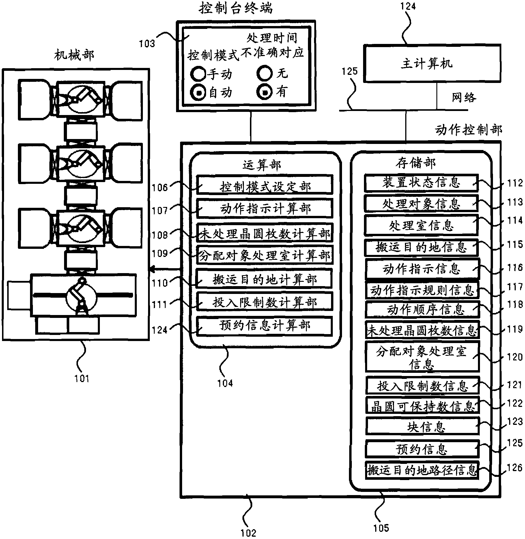
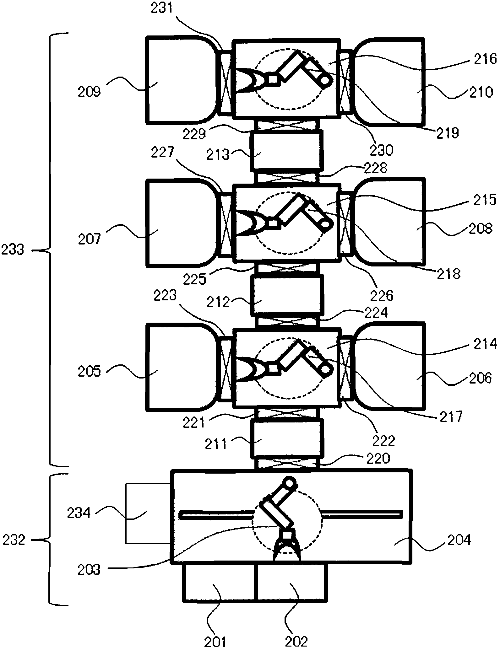
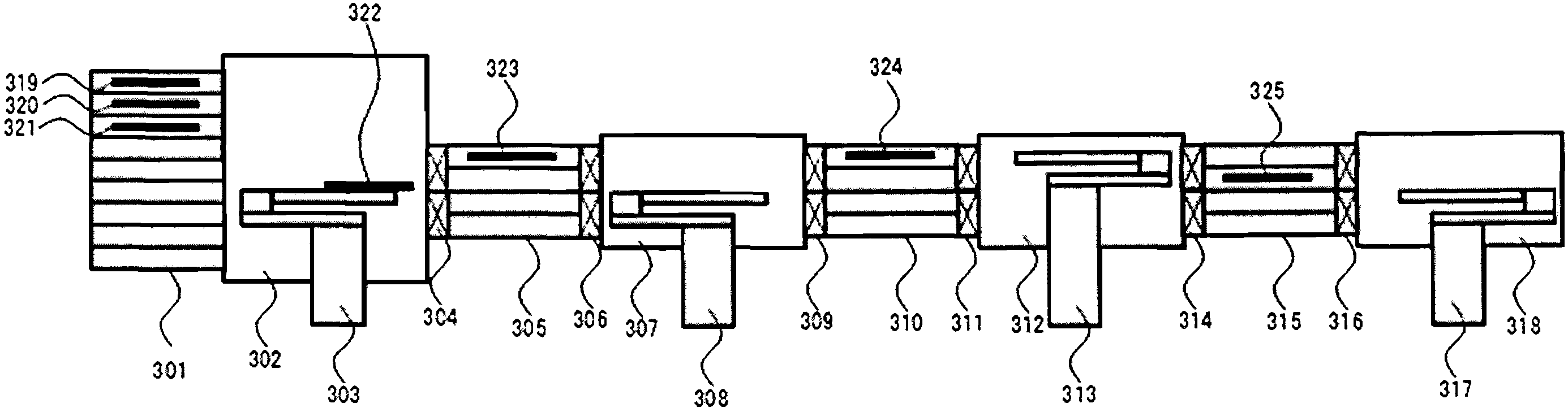
[0116] use figure 1 The outline of the overall configuration of the semiconductor processing apparatus of the present invention will be described. When roughly divided, the semiconductor processing apparatus is composed of a mechanical unit 101 including a processing chamber or a transfer mechanism, an operation control unit 102 , and a console terminal 103 . The mechanical unit 101 is composed of a processing chamber capable of performing processes such as etching and film formation on a wafer, and a transfer mechanism including a robot for transferring the wafer. The operation control unit 102 is a controller that controls the operation of the processing chamber or the transfer mechanism, and is composed of a calculation unit 104 that performs calculation processing and a storage unit 105 that stores various information. In the calculation unit 104, there is a control mode setting uni...


PUM


Abstract

An efficient method of controlling transportation in a linear tool type vacuum process device in a state that a length of time required for a process is not stable. For each process chamber, the number of unprocessed wafers that are in process or are being transported to the process chamber is counted, and in deciding a transport destination of a wafer, when the number of unprocessed wafers is equal to or larger than a charge limit amount, a transport destination of a wafer is decided excluding the process chamber. Also, a wafer holding mechanism on a transport path to a process chamber is reserved, and a transport destination of a processed member to be transported next is decided according to a status of reservation.

Description

technical field [0001] The present invention relates to a vacuum processing apparatus, and more particularly, to a method of transferring a semiconductor object to be processed (hereinafter referred to as a “wafer”) between processing chambers of the semiconductor processing apparatus. Background technique [0002] In a semiconductor processing apparatus, especially an apparatus that processes a processing object in a reduced-pressure apparatus, along with miniaturization and precision of processing, improvement in processing efficiency of a processing object wafer is required. For this reason, in recent years, a multi-chamber device in which a plurality of processing chambers are connected to one device has been developed, and the efficiency of productivity per unit installation area of ​​a clean room has been improved. In such an apparatus including a plurality of processing chambers for processing, the gas or pressure inside each clean room is regulated so as to be decomp...

Claims


Application Information

Patent Timeline
Patent Type & Authority Applications(China)
IPC IPC(8): H01L21/677H01L21/67
CPCH01L21/677H01L21/67H01L21/67276G05B2219/45032G05B19/41865Y02P90/02
Inventor 仲田辉男野木庆太井上智己川口道则
Owner HITACHI HIGH-TECH CORP
Learn More