Making method of semi-flexible printed circuit board

A technology for printed circuit boards and manufacturing methods, which is applied in the fields of printed circuit manufacturing, printed circuits, electrical components, etc., and can solve problems such as high difficulty in process control, high cost, and complicated process flow

Active Publication Date: 2012-11-28
KALEX MULTI LAYER CIRCUIT BOARD (ZHONGSHAN) CO LTD
View PDF6 Cites 12 Cited by
  • Summary
  • Abstract
  • Description
  • Claims
  • Application Information

AI Technical Summary

Problems solved by technology

However, in the manufacturing process of rigid-flexible printed circuit boards, there are disadvantages such as complex process flow, high difficulty in process control, low product reliability, and high cost.

Method used


Image

  • Making method of semi-flexible printed circuit board
  • Making method of semi-flexible printed circuit board
  • Making method of semi-flexible printed circuit board

Examples


Embodiment Construction

[0022] Embodiments of the present invention will be further described below in conjunction with the accompanying drawings.

[0023] The manufacturing method of the semi-flexible printed circuit board includes the following steps.

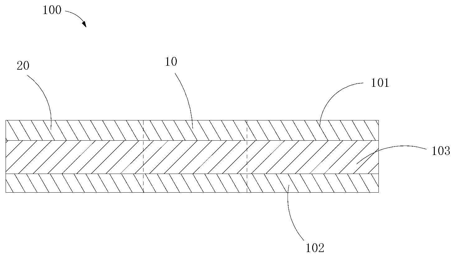
[0024] see figure 1 , providing an inner rigid circuit board. In this embodiment, the inner rigid circuit board 100 is a double-sided board and the circuit pattern has been prepared. Specifically, the inner rigid circuit board 100 includes a first circuit layer 101 , a second circuit layer 102 , and a first rigid insulating substrate 103 located between the first circuit layer 101 and the second circuit layer 102 . The inner rigid circuit board 100 is divided into a flexible area 10 and a non-flexible area 20, and the flexible area 10 is used for bending. In the fabrication of the first circuit layer 101 and the second circuit layer 102, steps such as material cutting, inner layer pattern transfer, etching and black oxidation are generally require...


PUM


Abstract

The invention provided a making method of a semi-flexible printed circuit board. The making method comprises the steps of: preparing an inner-layer rigid circuit board, wherein the inner-layer rigid circuit board is divided into a flexible region and a non-flexile region, and a circuit pattern is well made on the inner-layer rigid circuit board which is provided with a first circuit layer; laminating a layer of flexile insulation substrate and a first copper foil, wherein the flexible insulation substrate is located between the first circuit layer and the first copper foil; making a first outer-layer circuit on the first copper coil; printing first ink on the non-flexible region of the first outer-layer circuit to form a first soldermask layer, and printing second ink on the flexible region of the first outer-layer circuit to form a second soldermask layer; and removing a rigid part formed in the circuit board by using a routing process. In the making method provided by the invention, the second ink is printed in the flexible region, so that the problem that a solder resist cracks during board bending is solved. In the flexible region, the rigid layer is removed through depth control, a processing method is simple and a product is high in reliability.

Description

technical field [0001] The invention relates to the field of circuit boards, in particular to a method for manufacturing a semi-flexible printed circuit board. Background technique [0002] At present, with the rapid development of modern electronic technology, some electronic equipment needs to be bent repeatedly due to the compact space, large changes in high and low temperature environments, interconnection between components or possible multiple assembly and maintenance. Usually, in some applications (such as automotive electronics), continuous dynamic bending is not required, but only one or two bendings are required during installation, rework and repair. [0003] Existing technologies generally use rigid-flex circuit boards to meet this requirement. However, in the manufacturing process of rigid-flex printed circuit boards, there are disadvantages such as complex process flow, high difficulty in process control, low product reliability, and high cost. Contents of t...

Claims


Application Information

Patent Timeline
Patent Type & Authority Applications(China)
IPC IPC(8): H05K3/00
Inventor 陈德泉梁炳源
Owner KALEX MULTI LAYER CIRCUIT BOARD (ZHONGSHAN) CO LTD
Why Eureka
Try Eureka