

Transparent conductive element, input device, and display device
A technology of transparent conduction and transparent conduction layer, which is applied to optical elements, conduction layers on insulating carriers, input/output process of data processing, etc., can solve problems such as troublesome quality of display devices and input devices, and achieve small wavelength dependence Effect
Inactive Publication Date: 2012-11-28
DEXERIALS CORP
View PDF7 Cites 6 Cited by
- Summary
- Abstract
- Description
- Claims
- Application Information
AI Technical Summary
Problems solved by technology
For this reason, the reflectivity increases with the thickness of the transparent conductive layer, thus, it will cause trouble to the quality of the display device and the input device
Method used
View moreImage
Smart ImageViewing Examples

Examples
no. 1 approach
[0094] 1. First embodiment (an example in which the structure is configured as a transparent conductive element in a hexagonal lattice shape)
[0095] 2. Second embodiment (an example in which the structure is arranged as a transparent conductive element in a tetragonal lattice shape)
no. 3 approach
[0096] 3. The third embodiment (an example of a transparent conductive element in which the structure is randomly arranged)
[0097] 4. Fourth Embodiment (an example of a transparent conductive element in which a transparent conductive layer is continuously formed on the entire wave surface)
no. 5 approach
[0098] 5. Fifth Embodiment (First Application Example of Transparent Conductive Element Applied to Information Input Device)
Login to View More PUM
 Abstract
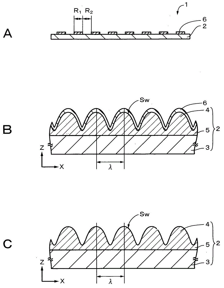
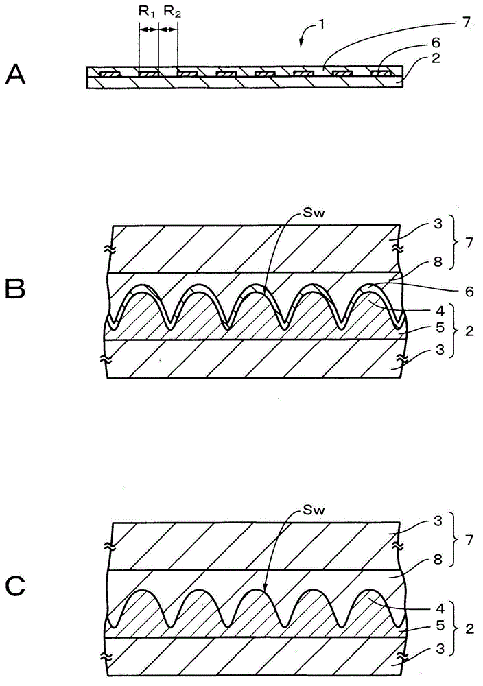
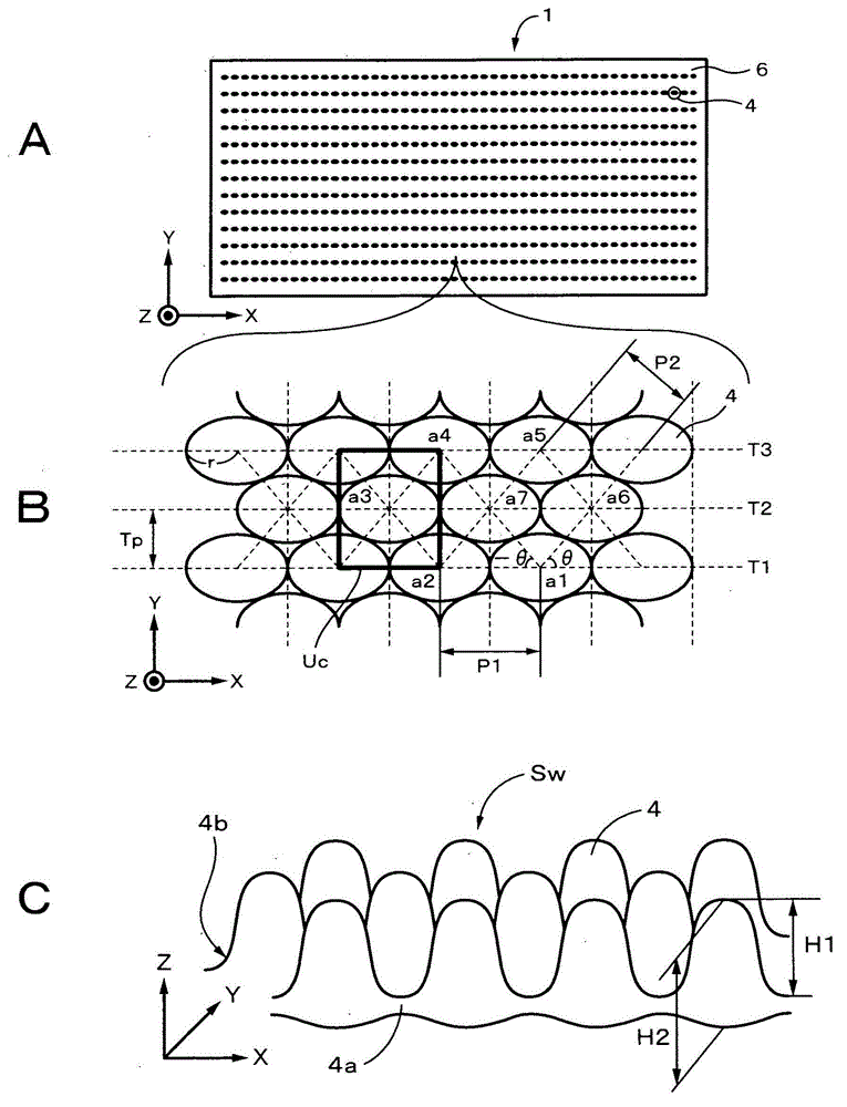
A transparent conductive element comprises: an optical layer wherein a wavefront is disposed, further comprising an average wavelength less than or equal to the wavelengths of visible light; and a transparent conductive layer which is formed upon the wavefront to follow the wavefront. With the average wavelength of the wavefront designated [lambda]m, and the average amplitude of the oscillation of the wavefront designated Am, the ratio (Am / [lambda]m) is greater than or equal to 0.2 and less than or equal to 1.0, the average wavelength of the wavefront [lambda]m is greater than or equal to 140 nm and less than or equal to 300 nm, the film thickness of the transparent conductive layer in the location where the wavefront is highest is 100 nm or less, the area of the flat part of the wavefront is 50% or less, and the reflected hue in the chromaticity scheme L*a*b* on the wavefront side is |a*| <= 10 and |b*| <= 10.
Description
technical field [0001] The invention relates to a transparent conductive element, an input device and a display device. In particular, the present invention relates to a transparent conductive element with anti-reflection function. Background technique [0002] Display devices such as electronic paper and input devices such as touch panels use transparent conductive materials in which a transparent conductive layer is formed on a plane of a base. Higher refractive index materials such as ITO (Indium Tin Oxide) are used as materials for transparent conductive layers used in transparent conductive elements, where the refractive index is approximately 2.0. For this reason, the reflectance increases with the thickness of the transparent conductive layer, and thus, this causes troubles in the quality of the display device and the input device. [0003] Generally, in order to improve the transmission characteristics of a transparent conductive element, a technique of forming an ...
Claims
Login to View More Application Information
Patent Timeline
 Patent Type & AuthorityApplications(China)
IPC IPC(8): G06F3/041
CPCB32B7/02G02B1/10G02F1/1333G06F1/1637G02F1/167H01B5/14G06F3/041G02B1/118G02B1/116
Inventor林部和弥梶谷俊一村本穣
OwnerDEXERIALS CORP