Array substrate row driving circuit, display panel and display device

A technology of array substrate rows and driving circuits, applied in static indicators, instruments, etc., to ensure stability and small fluctuations

Active Publication Date: 2014-10-15
BOE TECH GRP CO LTD
View PDF8 Cites 0 Cited by
  • Summary
  • Abstract
  • Description
  • Claims
  • Application Information

AI Technical Summary

Problems solved by technology

[0004] AMOLED technology based on low-temperature polysilicon technology, the thin-film transistors driving the panel have high mobility, so it is more conducive to the integration of GOA circuits. a bit less

Method used


Image

  • Array substrate row driving circuit, display panel and display device
  • Array substrate row driving circuit, display panel and display device
  • Array substrate row driving circuit, display panel and display device

Examples


Embodiment 1

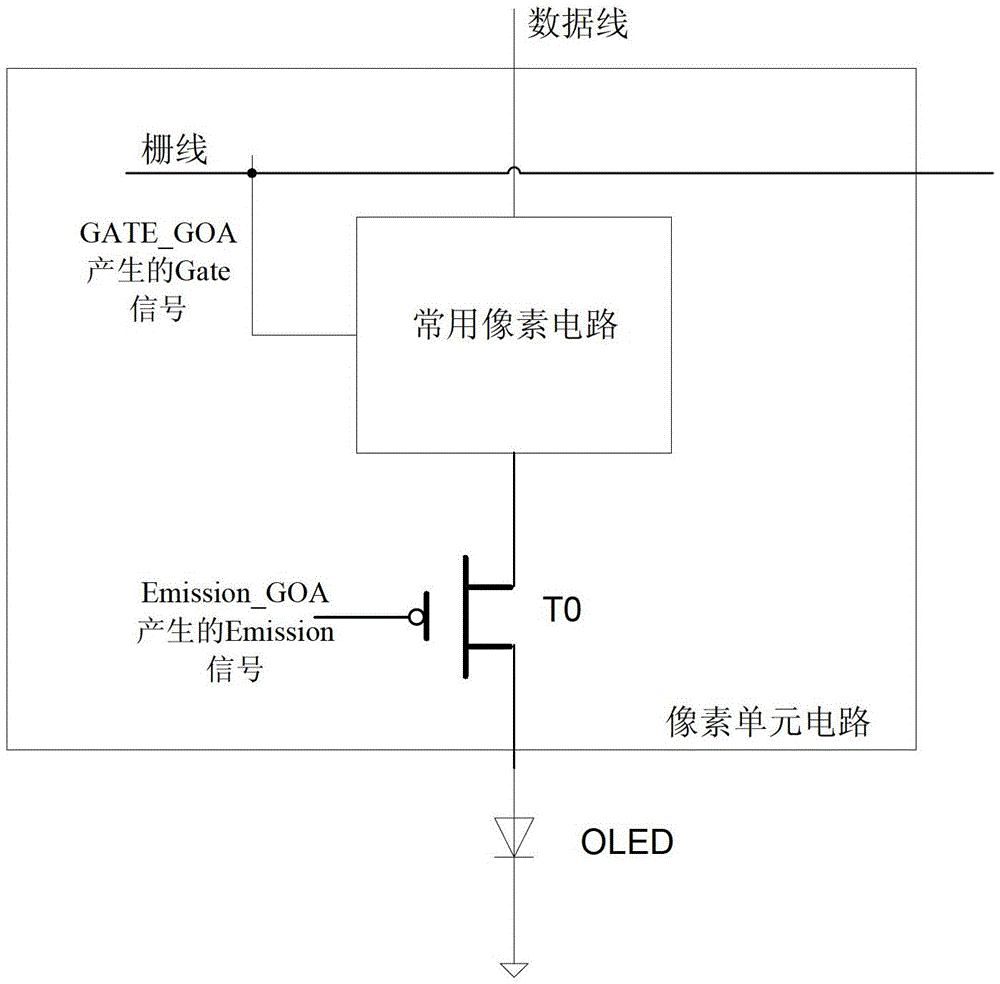
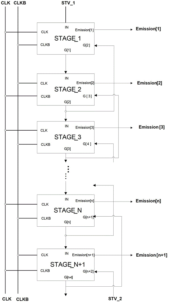
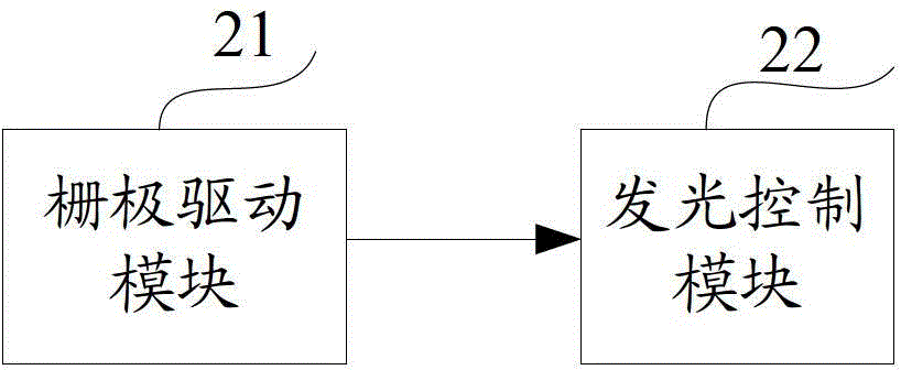
[0041] Embodiment 1 of the present invention provides a row driving circuit for an array substrate, the structure of which is shown in figure 2 As shown, it includes series-connected multi-stage circuit units STAGE_1~STAGE_N+1, and the structure of each stage circuit unit is as follows image 3 As shown, it includes a gate drive module 21 and a light emission control module 22, the gate drive module 21 is used to generate a gate drive signal, the light emission control module 22 and the gate drive signal output of the gate drive module 21 The terminal is connected, and is used to generate a light-emitting control signal for controlling the switch of the organic light-emitting diode under the control of the gate drive signal, and the gate drive signal and the light-emitting control signal are inverted.

Embodiment 2

[0043] Embodiment 2 of the present invention provides a row driving circuit for an array substrate, the structural diagram of which is shown in figure 2 As shown, on the basis of Embodiment 1, the gate drive module 21 includes the first thin film transistor T1 to the seventh thin film transistor T5 and the first bootstrap capacitor C1, wherein,

[0044] The first terminal of T1 is respectively connected to the third terminal of T5 and the second terminal of T4, the second terminal is connected to an external level signal, and the third terminal is connected to the second terminal of C1 and T2 respectively, and serves as the gate drive signal output;

[0045] The first terminal of T3 is connected to the clock signal CLK, the second terminal is respectively connected to the first terminals of T5, C1 and T2, and the third terminal is connected to the gate drive signal output terminal of the upper circuit unit;

[0046] The first terminal of T4 and the second terminal of T5 are ...

Embodiment 3

[0050] Embodiment 3 of the present invention provides a row driving circuit for an array substrate, the structural diagram of which is shown in figure 2 As shown, on the basis of the second embodiment, the gate drive module further includes thin film transistors T6 and T7, wherein the first terminal of T7 is connected to the reverse signal CLKB of the clock signal, and the second terminal is connected to the third terminal of T5 The third terminal is connected to the second terminal of T6 and the first terminal of T1 respectively; the first terminal of T6 is connected to the clock signal CLK, and the third terminal of T6 is connected to the second terminal of T4.

[0051] Transistors T6 and T7 are added to the circuit, which are connected in series with T4 and T5 respectively, so that the working state is more stable, and the connection relationship between the level of point N2 and the high and low levels is further clarified. For example, in the reset period t3, the transist...


PUM


Abstract

The invention relates to the technical field of display and discloses an array substrate row driving circuit, a display panel and a display device. The array substrate row driving circuit can generate control signals which precisely control OLED (organic light emitting diode) driving current to realize respective control of OLED device operating conditions and a pixel circuit, so that OLED flickering caused by instable pixel current when data are written into the pixel circuit is avoided. The driving circuit comprises a gate driving module and a light emitting control module, the gate driving module is used for generating gate driving signals, the light emitting control module is connected with a gate driving signal output end of the gate driving module and used for generating light emitting control signals which control on / off of organic light emitting diodes under control of the gate driving signals, and the gate driving signals and the light emitting control signals are opposite in phase.

Description

technical field [0001] The present invention relates to the field of display technology, in particular to an array substrate row driving circuit, a display panel and a display device. Background technique [0002] When the traditional passive matrix organic light-emitting diode (Passive Matrix OLED, PMOLED for short) is applied to the display, as the display size of the display increases, the driving time of a single pixel needs to be shorter, so the transient current needs to be increased. This increases power consumption. At the same time, the application of a large current will cause an excessive voltage drop on the ITO line, and make the OLED operating voltage too high, thereby reducing its efficiency. However, active matrix organic light-emitting diodes (Active Matrix OLED, AMOLED for short) can solve these problems well by inputting OLED current through row-by-row scanning of switching tubes. Therefore, AMOLED has been increasingly used in high-performance displays d...

Claims


Application Information

Patent Timeline
Patent Type & Authority Patents(China)
IPC IPC(8): G09G3/32G09G3/3225
Inventor 王颖金泰逵金馝奭
Owner BOE TECH GRP CO LTD
Why Eureka
Try Eureka