Current diffusion layer, light emitting diode device and manufacturing method thereof
A technology of light-emitting diodes and current diffusion layers, applied in circuits, electrical components, semiconductor devices, etc., can solve the problems of inability to uniformly diffuse current, reduce light extraction efficiency, and inability to uniformly diffuse, and achieve increased light extraction efficiency, reduced total reflection, The effect of uniform current spreading
- Summary
- Abstract
- Description
- Claims
- Application Information
AI Technical Summary
Problems solved by technology
Method used
Image

Examples
no. 1 example
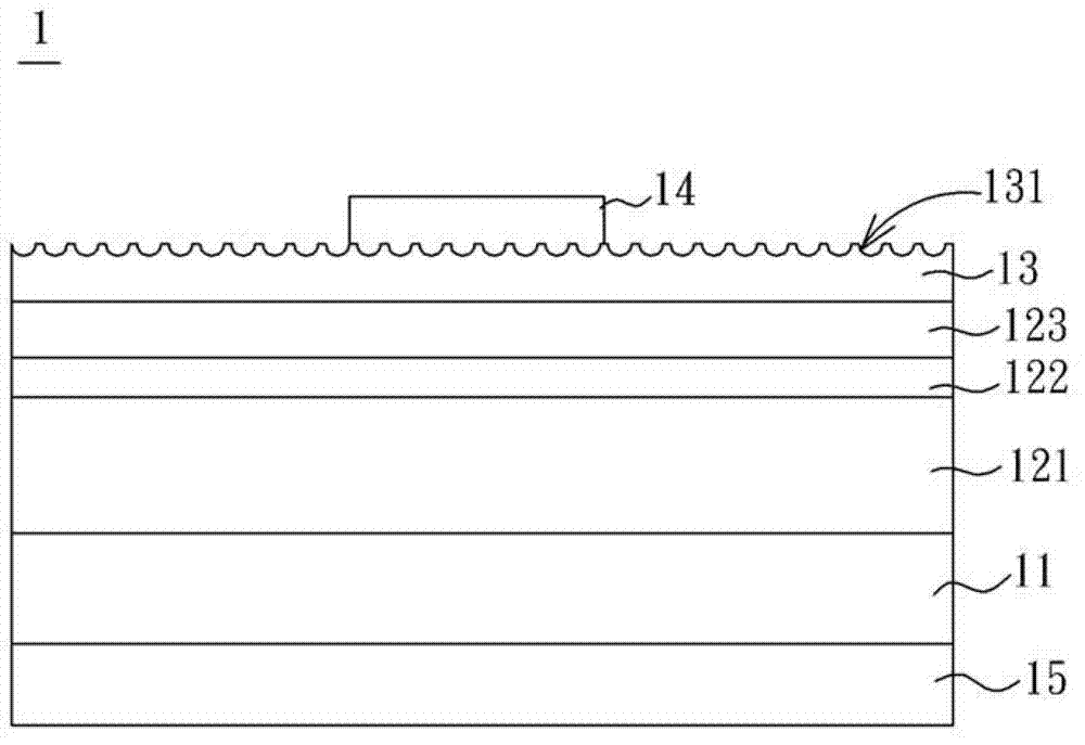
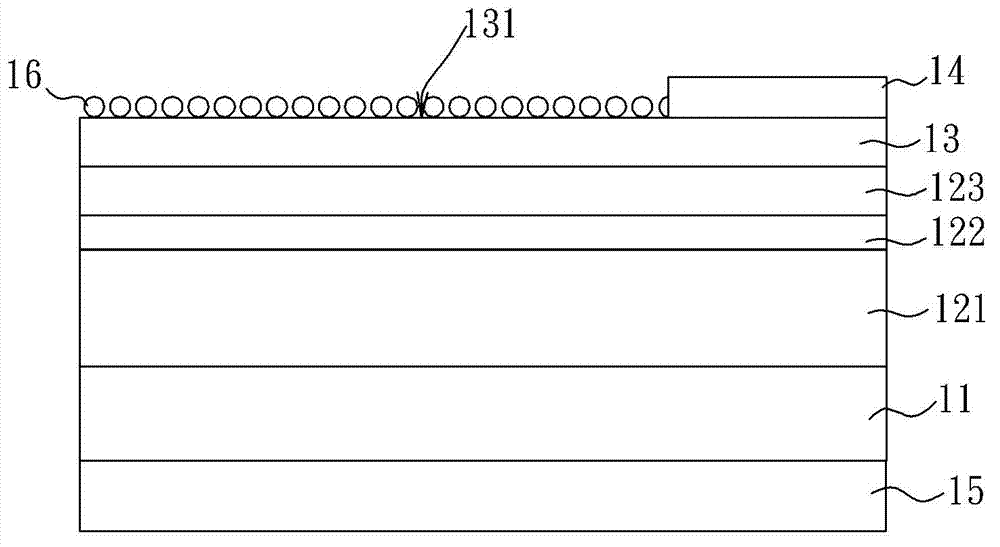
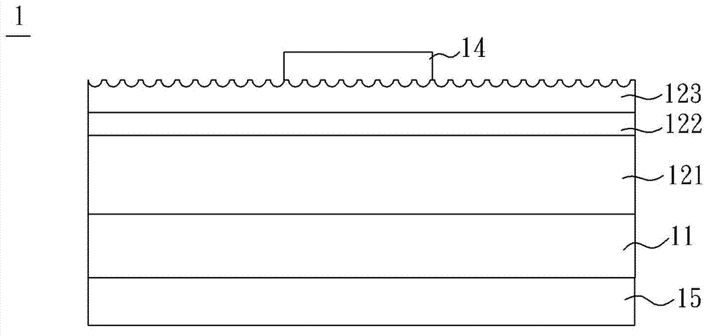
[0053] Please refer to image 3 , according to the first embodiment of the present invention, a method of manufacturing a light emitting diode device 20 includes step S11 to step S15. Please also refer to the following Figure 4A to Figure 4E shown.
[0054] Such as Figure 4A As shown, step S11 is to form an epitaxial stack 21 on the epitaxial substrate 211 , wherein the epitaxial stack 21 includes a first semiconductor layer 212 , a light emitting layer 213 and a second semiconductor layer 214 . The first semiconductor layer 212 is formed on the epitaxial substrate 211 , and then the light emitting layer 213 is formed on the first semiconductor layer 212 ; and then the second semiconductor layer 214 is formed on the light emitting layer 213 . Next, if Figure 4B As shown, step S12 is to remove part of the light emitting layer 213 and part of the second semiconductor layer 214 .
[0055] Such as Figure 4CAs shown, step S13 is to connect the current spreading layer 22 w...
no. 2 example
[0061] Please refer to Figure 5 , according to the second embodiment of the present invention, a method for manufacturing a light emitting diode device 30 includes steps S21 to S27. Please also refer to the following Figure 6A to Figure 6F.
[0062] like Figure 6A As shown, step S21 is the same as step S11 of the first embodiment, which forms the epitaxial stack 31 on the epitaxial substrate 311 . Wherein, the epitaxial stack 31 includes a first semiconductor layer 312 , a light emitting layer 313 and a second semiconductor layer 314 . The first semiconductor layer 312 is formed on the epitaxial substrate 311 , and then the light emitting layer 313 is formed on the first semiconductor layer 312 ; and then the second semiconductor layer 314 is formed on the light emitting layer 313 .
[0063] Step S22 connects the current spreading layer 32 to the epitaxial stack 31 . In this embodiment, the current spreading layer 32 is formed on the second semiconductor layer 314 by, ...
no. 3 example
[0072] Please refer to Figure 7 A method for manufacturing a light emitting diode device according to the third embodiment of the present invention includes steps S31 to S36. Please also refer to the following Figure 8A to Figure 8E .
[0073] like Figure 8A As shown, step S31 is the same as step S11 of the first embodiment, which forms an epitaxial stack 41 on the epitaxial substrate 111 . Wherein, the epitaxial stack 41 includes a first semiconductor layer 412 , a light emitting layer 413 and a second semiconductor layer 414 . The first semiconductor layer 412 is formed on the epitaxial substrate 411 , and then the light emitting layer 413 is formed on the first semiconductor layer 412 ; and then the second semiconductor layer 414 is formed on the light emitting layer 413 .
[0074] Step S32 is to connect the current spreading layer 42 with the epitaxial stack 41 . In this embodiment, the current spreading layer 42 is formed on the second semiconductor layer 414 by, ...
PUM
| Property | Measurement | Unit |
|---|---|---|
| Thermal conductivity | aaaaa | aaaaa |
| Thermal conductivity | aaaaa | aaaaa |
Abstract
Description
Claims
Application Information
 - Generate Ideas
- Intellectual Property
- Life Sciences
- Materials
- Tech Scout
- Unparalleled Data Quality
- Higher Quality Content
- 60% Fewer Hallucinations
Browse by: Latest US Patents, China's latest patents, Technical Efficacy Thesaurus, Application Domain, Technology Topic, Popular Technical Reports.
© 2025 PatSnap. All rights reserved.Legal|Privacy policy|Modern Slavery Act Transparency Statement|Sitemap|About US| Contact US: help@patsnap.com