Touch panel and touch display device

A technology of touch display device and touch panel, which is applied in optics, instrumentation, electrical digital data processing, etc., can solve the problems of large finger influence and large noise, and achieve the effects of enhancing performance, reducing noise, and improving sex-to-noise ratio

Active Publication Date: 2015-08-12
BOE TECH GRP CO LTD
View PDF2 Cites 2 Cited by
  • Summary
  • Abstract
  • Description
  • Claims
  • Application Information

AI Technical Summary

Problems solved by technology

[0003] like figure 2 and image 3 As shown, the peripheral wiring 111 is located at the edge of the touch panel surface. When touching the edge of the touch panel during use, because the finger is too close to the peripheral wiring 111, the influence of the finger on other channels is particularly large. generate loud noise

Method used


Image

  • Touch panel and touch display device
  • Touch panel and touch display device
  • Touch panel and touch display device

Examples


Embodiment 1

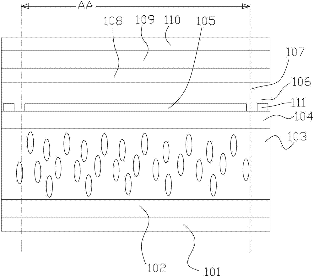
[0027] Such as Figure 4 As shown, this embodiment describes a touch panel, which includes a metal bridge 201, a first insulating layer 202, a touch electrode layer (ITO) 203, a second insulating layer 204, and a flat layer sequentially formed on a base substrate. (OC layer) 205, an upper polarizer 206 and a cover layer 207, a peripheral wiring 208 on the same layer as the metal bridge 201 is provided on the edge of the touch panel, the second insulating layer 204 and the OC layer 205 A guard electrode layer 209 covering the peripheral wiring 208 is formed therebetween.

[0028] It should be noted that, in Figure 4 2 only schematically shows different layer structures, and the connection relationship between the touch electrode layer 203 and the metal bridge 201 is not shown here.

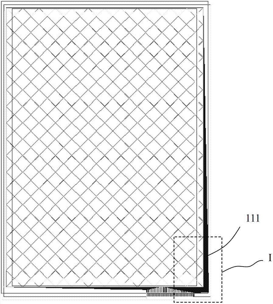
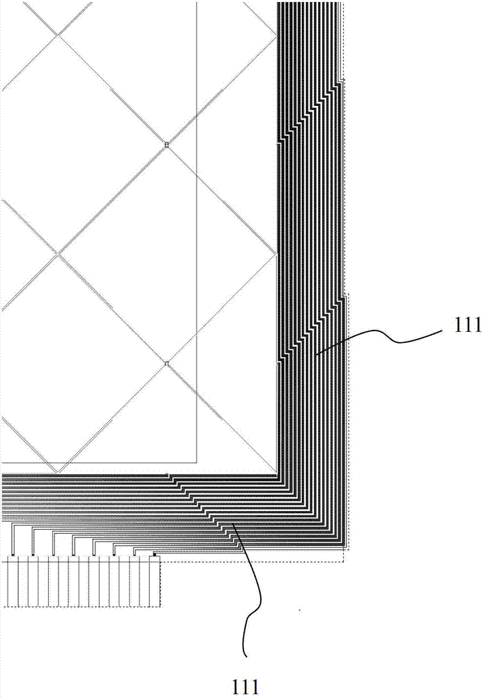
[0029] Such as Figure 5 with Image 6 As shown, in this embodiment, the protective electrode layer 209 is a rectangular frame structure, and the width W1 of the frame bar forming the frame st...

Embodiment 2

[0033] This embodiment describes a touch display device, which includes the touch panel described in the first embodiment. The touch display device may be, but not limited to, a liquid crystal touch display device; in addition, it may also be a touch display device based on display modes such as OLED (Organic Light Emitting Diode) display.

[0034] exist Figure 4 shows a liquid crystal touch display device, which includes the structures of the touch panel and the liquid crystal panel described in the first embodiment. In this embodiment, the liquid crystal panel includes a lower polarizer 210, an array substrate 211, a liquid crystal layer 212, and a color filter substrate 213 arranged in sequence. side. In other embodiments of the present invention, the liquid crystal panel can also add or subtract some layers, or have other different structures, as long as the liquid crystal display can be realized.

[0035] In the touch panel of this embodiment, when the user's finger t...


PUM


Abstract

The invention discloses a touch panel, which comprises a metallic bridge, a first insulating layer, a touch electrode layer, a second insulating layer, a flat layer and a cover plate layer which are sequentially formed on a substrate base plate. The edge of the touch panel is provided with peripheral wires which are positioned in the same layer with the metallic bridge, and a protective electrode layer covering the peripheral wires is formed between the second insulating layer and the flat layer. The invention also discloses a touch display device of the touch panel. The touch panel is provided with the protective electrode layer, so that noises caused by touching the edge of the touch panel are reduced, the signal-to-noise ratio of the touch panel is increased, and the performance of the touch panel is enhanced.

Description

technical field [0001] The present invention relates to the field of touch technology, in particular to a touch panel and a touch display device. Background technique [0002] In the existing touch panel technology, the on-cell touch display includes two parts: a liquid crystal panel and a touch panel, and its structure is as follows: figure 1 As shown, it includes a lower polarizer 101, an array substrate 102, a liquid crystal layer 103, a color filter substrate 104, a metal bridge 105, an insulating layer 106, a touch electrode layer 107 (including driving electrodes and sensing electrodes), and a flat Layer (Over Coat, OC) 108 , upper polarizer 109 and glass cover 110 . During processing, peripheral wiring 111 of metal material outside the display area (Active Area, AA) is fabricated on the same layer as the metal bridge 105 for connecting with the touch electrodes. Wherein, the touch electrode can be made of nano Indium Tin Oxides (ITO) material; moreover, in the touch...

Claims


Application Information

Patent Timeline
Patent Type & Authority Patents(China)
IPC IPC(8): G06F3/041G02F1/1333
Inventor 刘尧虎赵家阳
Owner BOE TECH GRP CO LTD
Why Eureka
Try Eureka