Capacitance multiplier

A capacitance multiplication and capacitance technology, which is applied to electrical components, networks using active components, impedance networks, etc., can solve problems affecting circuit noise performance, large area of ​​capacitance multiplier, and large ratio of chip area, etc., to improve noise Performance, fewer components, and less noise

Inactive Publication Date: 2012-12-19
INST OF MICROELECTRONICS CHINESE ACAD OF SCI
View PDF5 Cites 5 Cited by
  • Summary
  • Abstract
  • Description
  • Claims
  • Application Information

AI Technical Summary

Problems solved by technology

With the continuous reduction of process feature size, the area of ​​transistors is also continuously reduced, but the impact on the area of ​​passive devices is very small, which restricts the reduction of chip cost
[0003] To sum up, the current capacitor multiplier has a large area and occupies a large proportion of the entire chip area, which will increase the cost of the entire chip
At the same time, the circuit structure of the current capacitor multiplier using passive components is complex, therefore, it will affect the noise performance of the entire circuit

Method used


Image

  • Capacitance multiplier
  • Capacitance multiplier

Examples


Embodiment Construction

[0020] In order to make the above objects, features and advantages of the present invention more comprehensible, specific implementations of the present invention will be described in detail below in conjunction with the accompanying drawings.

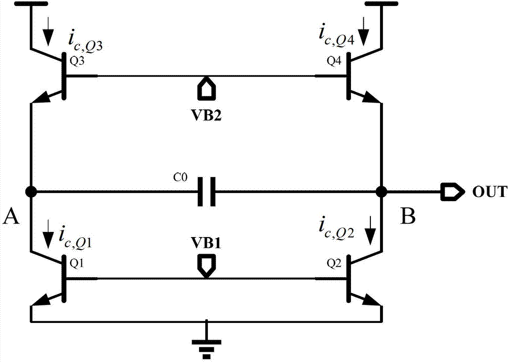
[0021] see figure 1 , which is a circuit diagram of Embodiment 1 of the capacitance multiplier provided by the embodiment of the present invention.

[0022] The capacitance multiplier provided in this embodiment includes: a first transistor Q1, a second transistor Q2, a third transistor Q3, a fourth transistor Q4, and a first capacitor C0;

[0023] The collector of the first transistor Q1 is connected to the first node A, the emitter is grounded, and the base is connected to the first bias voltage VB1;

[0024] The collector of the second transistor Q2 is connected to the second node B, the emitter is grounded, and the base is connected to the first bias voltage VB1;

[0025] The collector of the third transistor Q3 is connected to a...


PUM


Abstract

The invention provides a capacitance multiplier which employs an active device. Since the area of the active device is intrinsically smaller than that of a passive device, and the capacitance multiplier only comprises four transistors and a capacitor and is simple in structure, the capacitance multiplier is small in area, and cost of an integral chip can be reduced. Further, noise generated by the whole capacitance multiplier is low as devices are less, so that improvement of the noise performance of a whole circuit is benefited.

Description

technical field [0001] The invention relates to the technical field of integrated circuits, in particular to a capacitance multiplier. Background technique [0002] A capacitor multiplier can be applied to a loop filter in a Phase Locked Loop (PLL, Phase Locked Loop). Traditional loop filters use passive capacitors and resistors to design circuits. Under the requirements of PLL performance, the value of capacitors will be very large. If the loop filter is designed using the on-chip method, the process determines that the capacitor occupies a large area, exceeding 50% of the entire PLL area. With the shrinking of process feature size, the area of ​​transistors is also shrinking, but the impact on the area of ​​passive devices is very small, thus restricting the reduction of chip cost. [0003] To sum up, the current capacitor multiplier has a relatively large area and occupies a large proportion of the entire chip area, which will increase the cost of the entire chip. At t...

Claims


Application Information

Patent Timeline
Patent Type & Authority Applications(China)
IPC IPC(8): H03H11/00
Inventor 吕志强陈岚
Owner INST OF MICROELECTRONICS CHINESE ACAD OF SCI
Why Eureka
Try Eureka