CMOS image sensor module and manufacturing method thereof

A technology of image sensor and manufacturing method, which is applied in radiation control devices, semiconductor/solid-state device testing/measurement, etc., can solve the problems of low yield rate and high cost, and achieve low cost, stable performance, and good moisture-proof effect

Active Publication Date: 2016-03-16
GALAXYCORE SHANGHAI
View PDF1 Cites 0 Cited by
  • Summary
  • Abstract
  • Description
  • Claims
  • Application Information

AI Technical Summary

Problems solved by technology

[0011] The cost of the CMOS image sensor module formed by the prior art is high, and the yield rate is low

Method used


Image

  • CMOS image sensor module and manufacturing method thereof
  • CMOS image sensor module and manufacturing method thereof
  • CMOS image sensor module and manufacturing method thereof

Examples


no. 1 example

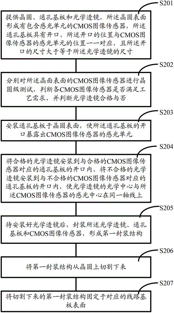
[0074] Please refer to figure 2 , the manufacturing method of the CMOS image sensor module in the first embodiment of the present invention, comprising:

[0075] Step S201, providing a wafer, a through-hole substrate, and an optical lens. A CMOS image sensor including a photosensitive unit is formed on the surface of the wafer. The through-hole substrate has an opening, and the position of the opening is the same as that of the photosensitive unit of the CMOS image sensor. The positions are in one-to-one correspondence, and the size of the opening is greater than or equal to the size of the optical lens;

[0076] Step S202, performing a wafer-level test on the CMOS image sensors on the wafer surface, judging whether each CMOS image sensor meets the process requirements, and judging whether the optical lens is qualified;

[0077] Step S203, installing a through-hole substrate on the surface of the wafer, so that the opening of the through-hole substrate exposes the photosensi...

no. 2 example

[0112]Different from the first embodiment of the present invention, in the second embodiment of the present invention, after the through-hole substrate is installed on the wafer surface to expose the photosensitive unit of the CMOS image sensor, a protective plate is formed on the surface of the through-hole substrate to protect the subsequent The CMOS image sensor in the process is protected from dust and moisture. And before installing the optical lens into the opening of the through-hole substrate, the protective plate is removed.

[0113] Please refer to Figure 7 , the manufacturing method of CMOS image sensor module in the second embodiment of the present invention, comprises:

[0114] Step S401, providing a wafer, a through-hole substrate, and an optical lens. A CMOS image sensor including a photosensitive unit is formed on the surface of the wafer. The through-hole substrate has an opening, and the position of the opening is the same as that of the photosensitive unit...

no. 3 example

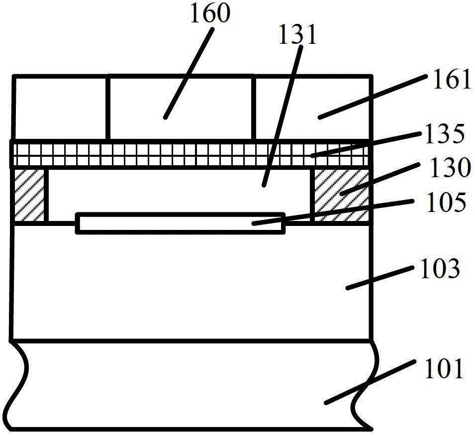
[0159] Different from the first embodiment and the second embodiment of the present invention, the third embodiment of the present invention provides a CMOS image sensor module.

[0160] Accordingly, please refer to Figure 13 , the inventor also provides a CMOS image sensor module, including:

[0161] Circuit substrate 601;

[0162] A CMOS image sensor 603 located on the circuit substrate 601 and electrically connected to the circuit substrate 601, the CMOS image sensor 603 including a photosensitive unit 605;

[0163] An optical lens 660, the optical lens 660 is located above the CMOS image sensor 603, and the optical center of the optical lens 660 is on the same axis as the photosensitive center of the photosensitive unit 605;

[0164] The through-hole substrate 630 between the CMOS image sensor 603 and the optical lens 660, the through-hole substrate 630 has an opening 631, and the light of the optical lens 660 is irradiated to the photosensitive unit of the CMOS image s...


PUM


Abstract

The invention relates to a CMOS (Complementary Metal Oxide Semiconductor) image sensor module and a manufacturing method thereof. The manufacturing method of the CMOS image sensor module comprises the following steps of: respectively carrying out wafer-level test on CMOS image sensors on the surfaces of crystal planes, judging whether each CMOS image sensor meets the process requirements and judging whether optical lenses are qualified or not; installing through hole substrates on the surfaces of wafers to ensure openings of the through hole substrates to be exposed out of photosensitive units of the CMOS image sensors; and installing the qualified optical lenses in the openings of the through hole substrates corresponding to the qualified CMOS image sensors and installing the unqualified optical lenses in the openings of the through hole substrates corresponding to the unqualified CMOS image sensors, so that the optical center of the optical lenses and the photosensitive center of the CMOS image sensors are on the same axis. The formed CMOS image sensor module has the advantages of high yield, low manufacturing cost and stable quality.

Description

technical field [0001] The invention relates to the field of image sensor packaging, in particular to a CMOS image sensor module and a manufacturing method thereof. Background technique [0002] An image sensor is a device that converts one-dimensional or two-dimensional optical information into electrical signals. Image sensors can be further divided into two different types: Complementary Metal Oxide Semiconductor (CMOS) image sensors and Charge Coupled Device (CCD) image sensors. Among them, the CMOS image sensor has wider applications than the CCD image sensor. A CMOS image sensor includes a photodiode for sensing radiated light and a CMOS logic circuit for processing the sensed light into electrical signal data. [0003] The CMOS module is composed of CMOS image sensors. Because the CMOS module has the advantages of simple structure, small size and convenient application, it has a wide range of uses. [0004] Please refer to figure 1 , a CMOS image sensor module of ...

Claims


Application Information

Patent Timeline
Patent Type & Authority Patents(China)
IPC IPC(8): H01L27/146H01L21/66
Inventor 邓辉夏欢
Owner GALAXYCORE SHANGHAI
Why Eureka
Try Eureka