Method for forming semiconductor device

A semiconductor and device technology, applied in the field of semiconductor device formation, can solve problems such as reducing the reliability of semiconductor devices, achieve the effects of reducing etching rate and etching damage, improving protection, and improving reliability

Active Publication Date: 2013-01-02
SEMICON MFG INT (SHANGHAI) CORP
View PDF3 Cites 9 Cited by
  • Summary
  • Abstract
  • Description
  • Claims
  • Application Information

AI Technical Summary

Problems solved by technology

[0006] However, after the actual epitaxial layer process, not only an epitaxial layer is formed in the PMOS area, but also an epitaxial layer of the same material as the epitaxial layer in the PMOS area may also be formed in the NMOS area, which reduces the reliability of the semiconductor device.

Method used


Image

  • Method for forming semiconductor device
  • Method for forming semiconductor device
  • Method for forming semiconductor device

Examples


Embodiment Construction

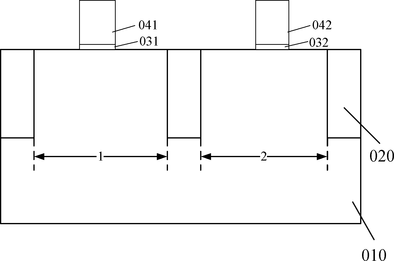
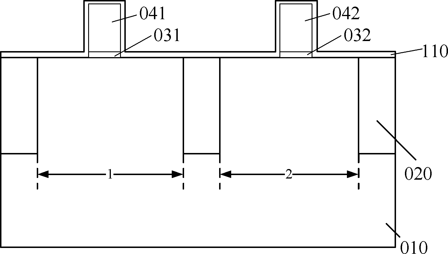
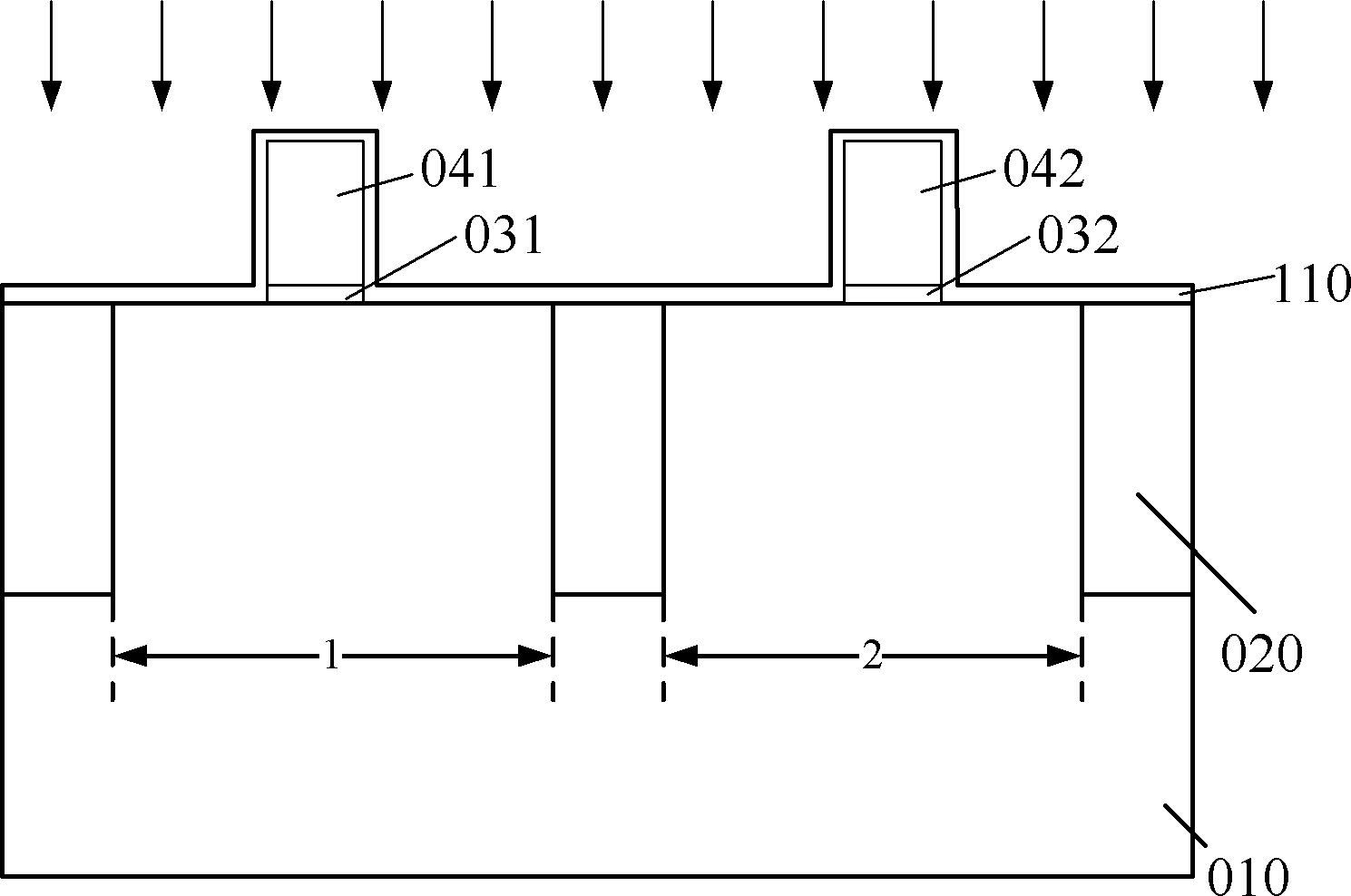
[0029] The inventors found that before forming the epitaxial layer, it is necessary to perform a series of dry etching, wet etching or cleaning processes on the above-mentioned semiconductor device. The above-mentioned processes will damage the sidewalls located in the NMOS region, so that the sidewalls of the NMOS region The walls thinned. The thinned sidewalls will not be able to provide better protection for the gate structure and the substrate, and even cause the NMOS gate structure and substrate to be exposed to the subsequent growth environment of the PMOS epitaxial layer, reducing the reliability of the NMOS device. Similarly, if the NMOS epitaxial layer is formed, the thinned sidewalls will not be able to protect the gate structure and the substrate well, and even cause the PMOS gate structure and substrate to be exposed to the subsequent NMOS epitaxial layer. In the growth environment, the reliability of the PMOS device is reduced.

[0030] In order to solve the abov...


PUM


Abstract

The invention discloses a method for forming a semiconductor device. The method includes that a substrate is provided, the substrate includes a first area and a second area, two gate structures which are located in the first area and the second area respectively are formed on the substrate, a first side wall and a second side wall are formed, the first side wall covers the substrate surface and two sides and surface of the gate structure in the first area, the second side wall covers the substrate surface and two sides and surface of the gate structure in the second area, the second side wall and the substrate are subjected to patterning etching, an opening is formed in the substrate which is located on two sides of the second side wall, an epitaxial layer is formed in the opening, before the epitaxial layer is formed, the first side wall is subjected to an ion implantation or an ion doping process, and thereby the density of the first side wall is improved. According to the method, the density of the first side wall is improved by the ion implantation or the ion doping process, and thereby the process selection ratio of the n-channel metal oxide semiconductor (NMOS) and the p-channel metal oxide semiconductor (PMOS) is improved when the epitaxial layer is formed on the same substrate.

Description

technical field [0001] The invention relates to the technical field of semiconductors, in particular to a method for forming a semiconductor device. Background technique [0002] It is well known that mechanical stress can change the energy gap and carrier mobility of silicon materials, and recently, mechanical stress has played an increasingly important role in affecting the performance of MOSFETs. If the stress can be properly controlled to increase the mobility of the carriers (electrons in n-channel transistors, holes in p-channel transistors) and drive current, stress can greatly improve the performance of transistors. [0003] Taking the PMOS transistor as an example, an epitaxial layer, such as a silicon germanium epitaxial layer, is first formed in the area where the source and drain regions need to be formed, and then doped to form the source and drain regions of the PMOS transistor. The silicon germanium epitaxial layer is formed to introduce The compressive stres...

Claims


Application Information

Patent Timeline
IPC IPC(8): H01L21/8238H01L21/265
Inventor 何永根
Owner SEMICON MFG INT (SHANGHAI) CORP
Why Eureka
Try Eureka