Liquid crystal display panel, substrate alignment method for liquid crystal display panel and substrate of liquid crystal display panel

A liquid crystal display panel and alignment direction technology, applied in the direction of instruments, nonlinear optics, optics, etc., can solve the problems of increasing the preparation time of alignment films, large alignment difference areas, and increasing production costs, so as to shorten the preparation time and reduce the Proportion, the effect of reducing production costs

Active Publication Date: 2013-01-09
SHANGHAI TIANMA MICRO ELECTRONICS CO LTD
View PDF6 Cites 12 Cited by
  • Summary
  • Abstract
  • Description
  • Claims
  • Application Information

AI Technical Summary

Problems solved by technology

But this will undoubtedly increase the production cost and increase the time for preparing the alignment film
[0017] In the prior art, when the alignment film is prepared on other substrates, the above-mentioned problems also exist. For example, the pixel electrodes on the array substrate also have a step difference area, so when the friction roller passes through the step difference area of ​​the pixel electrode, a relatively large alignment difference will also occur. region, eventually resulting in the occurrence of reverse twist domain malformation

Method used


Image

  • Liquid crystal display panel, substrate alignment method for liquid crystal display panel and substrate of liquid crystal display panel
  • Liquid crystal display panel, substrate alignment method for liquid crystal display panel and substrate of liquid crystal display panel
  • Liquid crystal display panel, substrate alignment method for liquid crystal display panel and substrate of liquid crystal display panel

Examples


Embodiment Construction

[0077] In order to make the above objects, features and advantages of the present invention more comprehensible, specific implementations of the present invention will be described in detail below in conjunction with the accompanying drawings.

[0078] In the following description, many specific details are set forth in order to fully understand the present invention, but the present invention can also be implemented in other ways than those described here, so the present invention is not limited by the specific embodiments disclosed below.

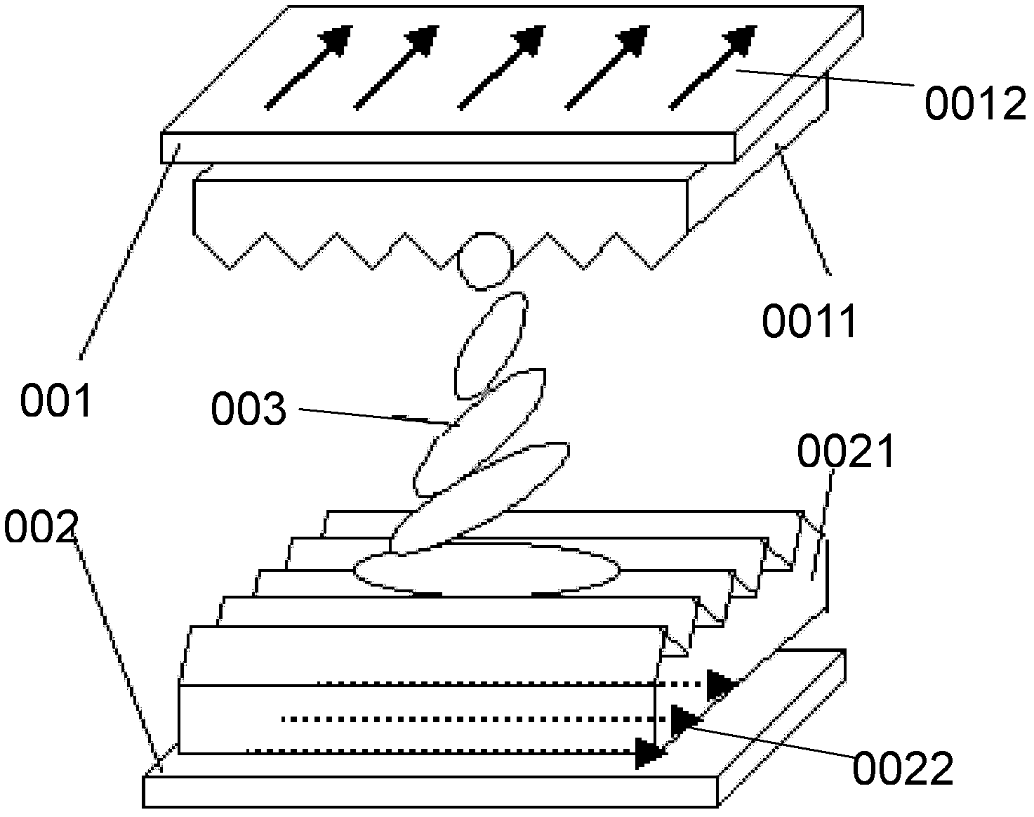
[0079] As mentioned in the background technology section, in the prior art, the alignment film of the substrate of the liquid crystal display panel is arranged on the upper layer of the device arranged in an array and has a step difference. During the rubbing process, when the friction roller passes through the step difference area of ​​the device, it will cause An alignment difference region of a certain area. When the proportion of the ...


PUM

PropertyMeasurementUnit
angleaaaaaaaaaa
angleaaaaaaaaaa
angleaaaaaaaaaa

Abstract

The invention relates to a liquid crystal display panel, a substrate alignment method for the liquid crystal display panel and a substrate of the liquid crystal display panel. The substrate alignment method includes the steps: providing the substrate provided with a plurality of arrayed devices; arranging alignment films on upper layers of the devices; rubbing the alignment films along the alignment direction of the substrate by friction rollers to form grooves on the alignment films; and enabling the included angle between one side of each device and the alignment direction of the substrate to be larger than or equal to 0 degree and smaller than 45 degrees. The poor occurring rate of a reverse twisting domain is reduced, light leak of a pixel black state / grey state is avoided, production cost is reduced, and preparation time of the alignment films is shortened.

Description

technical field [0001] The invention relates to the technical field of liquid crystal display, in particular to a substrate alignment method of a liquid crystal display panel, a substrate of a liquid crystal display panel and a liquid crystal display panel. Background technique [0002] Liquid crystal displays are widely used in various fields due to their small size, light weight, and low radiation. [0003] The liquid crystal display panel is the most important component of the liquid crystal display. The working principle of the liquid crystal display is: by changing the voltage applied to the liquid crystal to change the deflection angle of the liquid crystal molecules, thereby controlling the rotation direction and polarization state of the polarized light, so as to realize the change of the display state of the liquid crystal display. For example, the structure of a thin film field effect transistor liquid crystal display panel mainly includes: a color filter substrat...

Claims


Application Information

Patent Timeline
Patent Type & Authority Applications(China)
IPC IPC(8): G02F1/1337G02F1/1335
Inventor 陈文杰赵奇峰陈次文张世晓
Owner SHANGHAI TIANMA MICRO ELECTRONICS CO LTD
Why Eureka
Try Eureka