Infrared detection device and manufacturing method thereof

An infrared detection and semiconductor technology, which is applied in microstructure devices, manufacturing microstructure devices, decorative arts, etc., can solve the problem of high cost, and achieve the effect of improving sensitivity and overcoming pixel area.

Active Publication Date: 2016-12-21
SHANGHAI INTEGRATED CIRCUIT RES & DEV CENT
View PDF7 Cites 0 Cited by
  • Summary
  • Abstract
  • Description
  • Claims
  • Application Information

AI Technical Summary

Problems solved by technology

[0005] The technical problem to be solved by the present invention is to provide an infrared detection device and its manufacturing method to solve the problem of high cost caused by using sensitive materials for infrared detection in the prior art.

Method used


Image

  • Infrared detection device and manufacturing method thereof
  • Infrared detection device and manufacturing method thereof
  • Infrared detection device and manufacturing method thereof

Examples


Embodiment Construction

[0038] The implementation of the present invention will be described in detail below in conjunction with the drawings and examples, so that the realization process of how to use technical means to solve technical problems and achieve technical effects in the present invention can be fully understood and implemented accordingly.

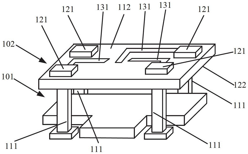
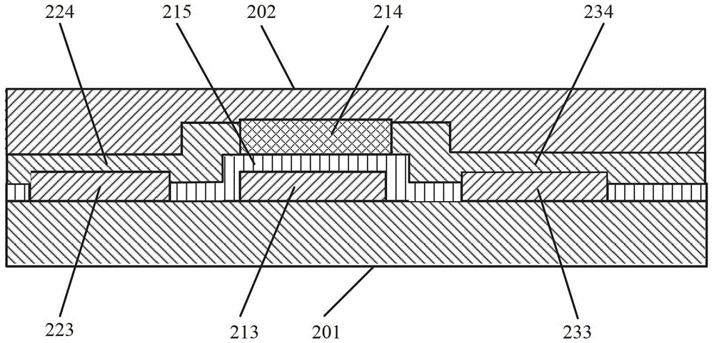
[0039] figure 1 It is a three-dimensional schematic diagram of an embodiment of the infrared detection device of the present invention. Such as figure 1 As shown, the infrared detection device in this embodiment includes: a micro-bridge structural unit 101 and a detection structural unit 102, the detection structural unit is arranged on the micro-bridge structural unit 101, and the detection structural unit 102 includes the first The release protection layer 112, the second release protection layer 122, and the transistor (not shown) arranged between the first release protection layer 112 and the second release protection layer 122; the transistor ...


PUM


Abstract

The invention discloses an infrared detection device and a manufacturing method thereof and belongs to the field of semiconductor devices. The infrared detection device comprises a microbridge structure unit and a detection structure unit which is arranged on the microbridge structure unit; the detection structure unit comprises a first release protection layer and a second release protection layer which are sequentially arranged on the microbridge structure unit from the bottom up, and a transistor which is arranged between the first release protection layer and the second release protection layer; the transistor comprises electrode layers and semiconductor layers; a grid electrode, a source electrode, and a drain electrode in each electrode layer are positioned on the same layer; and the semiconductor layers comprise a grid semiconductor layer which corresponds to the grid electrodes in the electrode layers, a source electrode semiconductor layer which corresponds to the source electrodes in the electrode layers and a drain electrode semiconductor layer which corresponds to the drain electrodes in the electrode layers.

Description

technical field [0001] The invention belongs to the field of semiconductor devices, and in particular relates to an infrared detection device and a manufacturing method thereof. Background technique [0002] Micro Electro Mechanical Systems (MEMS) technology has many advantages such as tiny, intelligent, executable, integrable, good process compatibility, and low cost, so it has been widely used in many fields including the field of infrared detection technology. Infrared detection device is a specific MEMS product in the field of infrared detection technology. It uses sensitive material detection layers such as amorphous silicon or vanadium oxide to absorb infrared rays, thereby causing changes in its resistance, and thereby realizing thermal imaging functions. . [0003] Figure 12 It is a structural schematic diagram of an infrared detection device in the prior art. Such as Figure 12 As shown, the infrared detection device in the prior art consists of a heat-sensitive ...

Claims


Application Information

Patent Timeline
Patent Type & Authority Patents(China)
IPC IPC(8): B81B7/02B81C1/00G01J5/20
Inventor 康晓旭
Owner SHANGHAI INTEGRATED CIRCUIT RES & DEV CENT
Why Eureka
Try Eureka