Pixel structure and manufacturing method for the pixel structure

一种画素结构、制作方法的技术,应用在半导体/固态器件制造、仪器、半导体器件等方向,能够解决画素结构解析度难以提升、电容电极与漏极短路、关键尺寸不易控制等问题,达到提升解析度与开口率、避免短路、减少光罩数目的效果

Inactive Publication Date: 2014-09-03
AU OPTRONICS CORP
View PDF4 Cites 0 Cited by
  • Summary
  • Abstract
  • Description
  • Claims
  • Application Information

AI Technical Summary

Problems solved by technology

As a result, a short circuit occurs between the capacitor electrode and the drain
In order to avoid the above situation, it is necessary to increase the distance between the capacitive electrode and the edge of the first opening of the flat layer by means of overexposure, etc., which may make it difficult to control the critical dimensions and improve the resolution of the pixel structure.

Method used


Image

  • Pixel structure and manufacturing method for the pixel structure
  • Pixel structure and manufacturing method for the pixel structure
  • Pixel structure and manufacturing method for the pixel structure

Examples


Embodiment Construction

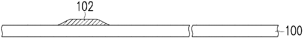
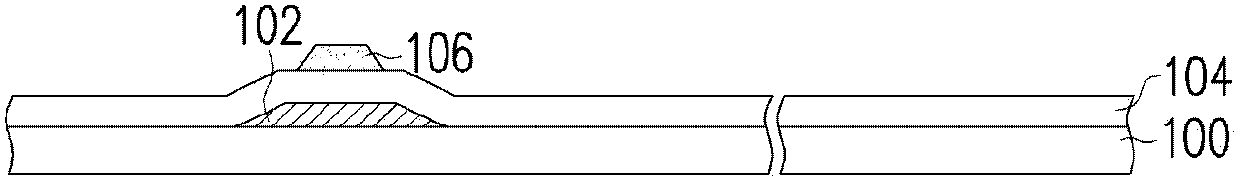
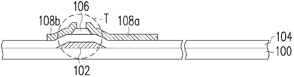
[0054] Figure 1A to Figure 1J It is a schematic flowchart of a method for manufacturing a pixel structure according to an embodiment of the present invention, Figure 2A for Figure 1J The schematic diagram of the top view, where Figure 1J The left part and right part of the ellipsis line are respectively along Figure 2A A schematic cross-sectional view of line A-A' and line B-B', and Figure 2B for Figure 2A An enlarged schematic view of the first to fourth openings of . First, please refer to Figure 1A to Figure 1D , forming a thin film transistor T on a substrate 100, and the thin film transistor T includes a first electrode 108a. In this embodiment, the substrate 100 includes, for example, an active area and a peripheral area (not shown), wherein Figure 1A to Figure 1J The described steps are performed on the substrate 100 in the active area. The thin film transistor T is, for example, a bottom gate (Bottom Gate) type thin film transistor, and its manufacturing...


PUM


Abstract

A pixel structure and a manufacturing method of the pixel structure. Firstly, an insulating layer and a planar layer are formed on the electrode, and the planar layer has a first opening to expose the insulating layer on the electrode. A conductive layer is formed on the planar layer, and the conductive layer is filled into the first opening. A patterned photoresist layer is formed with etched openings exposing the conductive layer above the electrodes. Using the patterned photoresist layer as a mask, perform a wet etching process on the conductive layer, remove the conductive layer on the electrode through the etching opening, and laterally etch the conductive layer under the patterned photoresist layer to form a second opening. The conductive layer is patterned, and the second opening is located in the first opening, exposing the insulating layer above the electrode. The patterned photoresist layer is used as a mask, and the insulating layer is subjected to a dry etching process, and the insulating layer above the electrode is removed through the etching opening to form a patterned insulating layer with a third opening that exposes the electrode. The third opening is smaller than The second opening is self-aligned with the second opening.

Description

【Technical field】 [0001] The present invention relates to a pixel structure and a manufacturing method of the pixel structure, and in particular to a high-resolution pixel structure and a manufacturing method of the pixel structure. 【Background technique】 [0002] Generally speaking, a pixel structure of a high-resolution display includes a thin film transistor and a pixel electrode electrically connected to the thin film transistor. The thin film transistor is configured on the substrate, including gate, gate dielectric layer, channel layer, source and drain. Generally, a thick flat layer is used to improve the flatness and make the liquid crystal rotate more smoothly. The flat layer is disposed on the substrate and has a first opening exposing part of the drain. The capacitor electrode is arranged on the planar layer and filled into the first opening, and the capacitor electrode has a second opening exposing the drain. The patterned insulating layer is disposed on the ca...

Claims


Application Information

Patent Timeline
Patent Type & Authority Patents(China)
IPC IPC(8): H01L21/77H01L27/12
CPCH01L29/6675H01L27/1288G02F1/134363H01L29/78663G02F1/136227H01L27/1248G02F1/136213H01L29/78654
Inventor 黄国有张玮伦陈茂松
Owner AU OPTRONICS CORP
Why Eureka
Try Eureka