Array substrate and manufacturing method thereof and LCD panel

A technology of an array substrate and a manufacturing method, applied in the field of liquid crystal display, can solve the problem of low utilization rate of substrate space, and achieve the effects of saving area, improving resolution, and improving utilization rate

Active Publication Date: 2013-01-16
BOE TECH GRP CO LTD +1
View PDF4 Cites 13 Cited by
  • Summary
  • Abstract
  • Description
  • Claims
  • Application Information

AI Technical Summary

Problems solved by technology

[0005] The array substrate, its manufacturing method, and liquid crystal display panel provided by the embodiments of the present invention are used to solve the technical problem of low space utilization of the substrate in the existing array substrate

Method used


Image

  • Array substrate and manufacturing method thereof and LCD panel
  • Array substrate and manufacturing method thereof and LCD panel
  • Array substrate and manufacturing method thereof and LCD panel

Examples


Embodiment Construction

[0035] The technical solutions in the embodiments of the present invention will be clearly and completely described below in conjunction with the accompanying drawings in the embodiments of the present invention. Obviously, the described embodiments are only a part of the embodiments of the present invention, rather than all the embodiments. Based on the embodiments of the present invention, all other embodiments obtained by those of ordinary skill in the art without creative work shall fall within the protection scope of the present invention.

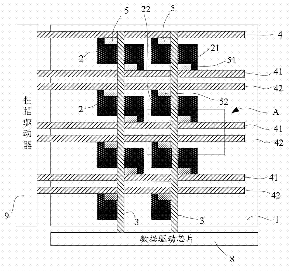
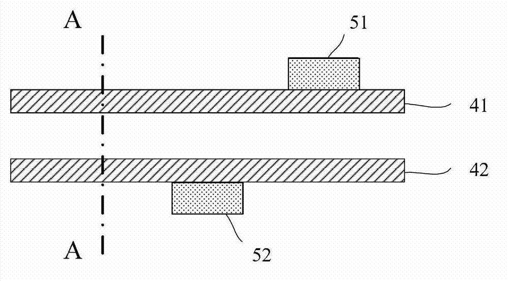
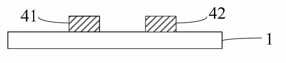
[0036] Such as Figure 4 , Figure 5 with Image 6 As shown, a specific embodiment of the array substrate provided by the present invention includes: a substrate 1; a plurality of sub-pixel groups located on the substrate 1, and each sub-pixel group includes first sub-pixels respectively arranged in two adjacent rows 2a and the second sub-pixel 2b, each first sub-pixel 2a includes a first thin film transistor 5a, and each second sub-pixel...


PUM


Abstract

The embodiment of the invention discloses an array substrate and a manufacturing method thereof and an LCD (Liquid Crystal Display) panel, which relates to the technical field of LCDs, and is invented to solve the technical problem of low substrate utilization in an existing array substrate. The array substrate comprises a substrate, wherein a first sub-pixel and a second sub-pixel are located on the substrate and respectively arranged in two adjacent rows; the first sub-pixel includes a first thin film transistor; the second sub-pixel includes a second thin film transistor; a first grid line and a second grid line are respectively arranged between the first sub-pixel and the second sub-pixel; the first grid line is used for applying grid electrode breakover voltage to the first thin film transistor; the second grid line is used for applying grid electrode breakover voltage to the second thin film transistor; a plurality of data lines crossed with the first grid line and the second grid line are used for applying data voltage to the first sub-pixel and the second sub-pixel through the same data line; and the first grid line and the second grid line are overlapped in an up-and-down manner in the direction perpendicular to the substrate, and the middle is separated by an insulating layer. The invention is used for a liquid crystal display device.

Description

Technical field [0001] The present invention relates to the field of liquid crystal display technology, in particular to an array substrate and a manufacturing method thereof, and a liquid crystal display panel. Background technique [0002] Thin film transistor liquid crystal display (TFT-LCD) is one of the most widely used flat panel displays. TFT-LCD generally includes a liquid crystal display panel, a scan driving circuit, and a data driving circuit. Among them, the liquid crystal display panel includes a color filter substrate and an array substrate arranged in a cell, and a liquid crystal layer sandwiched between the two substrates. The scan driving circuit and the data driving circuit are respectively connected to the TFT switch elements on the array substrate. [0003] Such as figure 1 , figure 2 with image 3 Shown is a structural schematic diagram of an array substrate with a double-gate line structure provided by the prior art, which includes a substrate 1, an array of...

Claims


Application Information

Patent Timeline
Patent Type & Authority Applications(China)
IPC IPC(8): H01L27/02H01L29/786H01L21/77G02F1/1362G02F1/1368
Inventor 孟庆超周保全
Owner BOE TECH GRP CO LTD
Why Eureka
Try Eureka