Manufacturing method of memory

A manufacturing method and memory technology, applied in the field of memory, can solve problems such as difficulty in further improving memory element characteristics, affecting peripheral area element characteristics, gate characteristic degradation, etc., and achieve the effect of enhanced and good element characteristics

Active Publication Date: 2013-01-30
WINBOND ELECTRONICS CORP
View PDF3 Cites 5 Cited by
  • Summary
  • Abstract
  • Description
  • Claims
  • Application Information

AI Technical Summary

Problems solved by technology

[0003] However, taking flash memory as an example, when performing a self-aligned contact window process or a self-aligned floating gate process on the memory cell region, it must be considered that these two processes themselves have complicated processes for the surrounding device regions. The thermal process used may affect the device characteristics of the peripheral area, such as the deterioration of the gate characteristics, or the boron penetration (boron penetration) effect in the gate oxide layer, so the temperature of the thermal process and other parameters should be adjusted.
That is to say, in order to take into account the element characteristics of the peripheral region, it may be necessary to sacrifice the better process conditions of the elements in the memory cell region, so it is difficult to further improve the element characteristics of the memory

Method used


Image

  • Manufacturing method of memory
  • Manufacturing method of memory
  • Manufacturing method of memory

Examples


Embodiment Construction

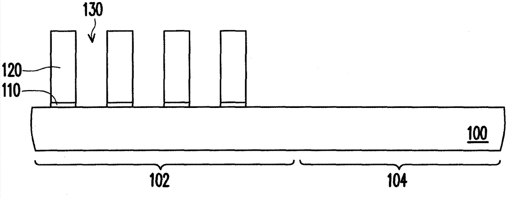
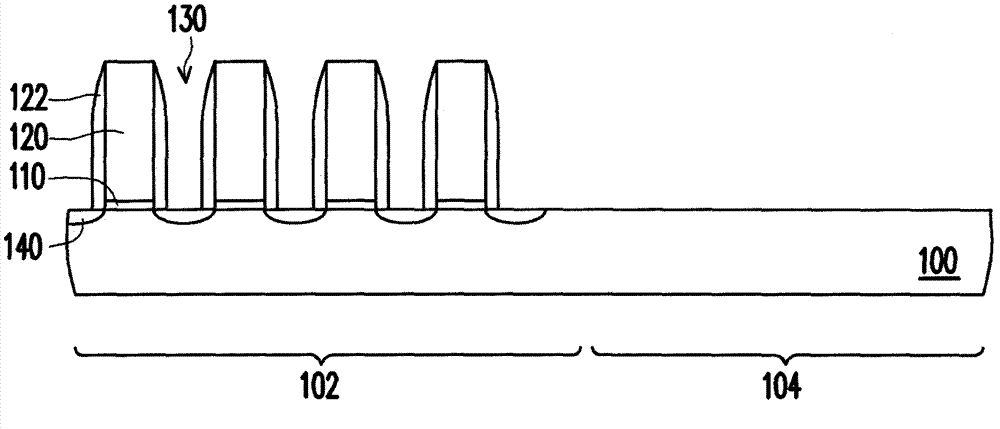
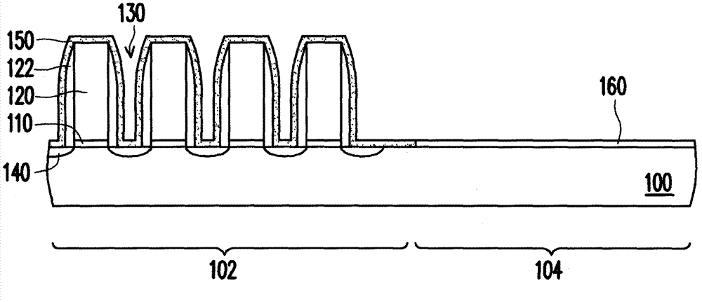
[0021] Figure 1A to Figure 1I It is a schematic cross-sectional view of a process of a method for manufacturing a memory according to an embodiment of the present invention.

[0022] Please refer to Figure 1A First, a substrate 100 is provided. The substrate 100 includes a memory cell region 102 and a peripheral region 104, wherein the memory cell region 102 is formed with a plurality of first gates 120 with a plurality of first openings 130 between the first gates 120. In this embodiment, it further includes forming a gate dielectric layer 110 between each first gate 120 and the substrate 100. The substrate 100 is, for example, a semiconductor substrate, such as an N-type or P-type silicon substrate, a group three or five semiconductor substrate, and the like. The gate dielectric layer 110 has, for example, a silicon oxide / silicon nitride / silicon oxide (ONO) structure. The material of the first gate 120 is, for example, doped polysilicon.

[0023] Please refer to Figure 1B The...


PUM


Abstract

The invention a manufacturing method of a memory, which comprises the following steps: providing a substrate, wherein the substrate comprises a memory cell zone and a perimeter zone, wherein a plurality of first grids are formed in the memory cell zone, and a plurality of first openings are arranged among the first grids; forming a nitride layer on the substrate in the memory cell zone, wherein the nitride layer is covered on the first grids and the first openings; forming an oxide layer on the substrate in the perimeter zone; carrying out a nitridizing technique to nitridize the oxide layer into a nitridized oxide layer; and forming a conductor layer on the substrate, wherein the conductor layer comprises a coverage layer positioned on the substrate in the memory cell zone and a plurality of plate grids positioned on the substrate in the perimeter zone, and the coverage layer is covered on the nitride layer and fully filled in the first openings.

Description

Technical field [0001] The present invention relates to memory technology, and more particularly to a method of manufacturing a memory. Background technique [0002] Generally speaking, as the size of flash memory gradually shrinks, in order to overcome the increasingly smaller line width and prevent misalignment, self-aligned contact (SAC) is used in the memory cell area. ) Process and self-aligned floating gate (SAF) process. [0003] However, taking the flash memory as an example, when the self-aligned contact window process or the self-aligned floating gate process is performed on the memory cell area, it must be considered that the two processes themselves have complex processes on the peripheral device area. The thermal process and the thermal process used may affect the device characteristics in the peripheral area, such as the deterioration of the gate characteristics, or the boron penetraion effect in the gate oxide layer, so the thermal process temperature and other para...

Claims


Application Information

Patent Timeline
Patent Type & Authority Applications(China)
IPC IPC(8): H01L21/28H01L21/8247
Inventor 廖修汉蒋汝平
Owner WINBOND ELECTRONICS CORP
Why Eureka
Try Eureka