Semiconductor laser element and manufacturing method of the same
A semiconductor and laser technology, applied in the field of semiconductor laser components and their manufacturing, can solve the problems of deteriorating performance, difficult to achieve high output, etc., and achieve the effect of accelerating heat dissipation
- Summary
- Abstract
- Description
- Claims
- Application Information
AI Technical Summary
Problems solved by technology
Method used
Image

Examples
Embodiment Construction
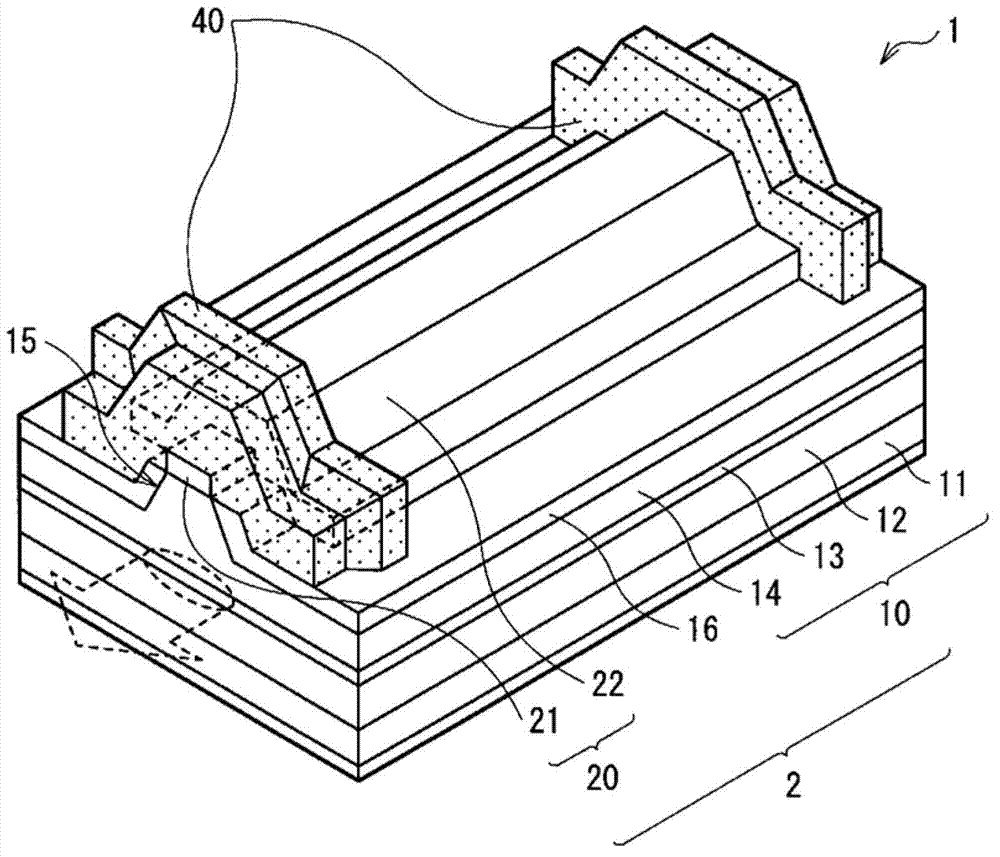
[0035] Hereinafter, a detailed description will be given of preferred embodiments of the present disclosure with reference to the accompanying drawings. It should be noted that the description will be given in the following order.
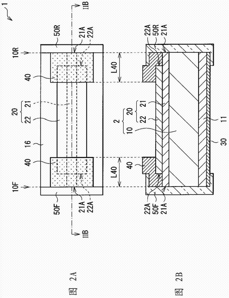
[0036] 1. Embodiment (Example in which non-metallic films are provided near the edges of two resonators on the top side of the p-side electrode)
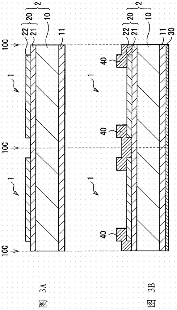
[0037] 2. Modification 1 (Example where a non-metallic film extends from one of the resonator edges to the other)
[0038] 3. Modification 2 (Example in which a non-metallic film is provided near one of the resonator edges)
[0039] 4. Modification 3 (Example in which the non-metallic film has an in-plane shape with no acute angle)
[0040] 5. Modification 4 (example in which the nonmetallic film has a shape divided in the in-plane direction)
[0041] 6. Modification 5 (example in which the thickness of the non-metallic film varies along the in-plane direction)
[0042] 7. Modification 6 (Example in ...
PUM
 Abstract
Description
Claims
Application Information