Double-sided circuit board structure

A double-sided circuit board and circuit board technology, which is applied in the direction of circuits, printed circuits connected with non-printed electrical components, electrical components, etc., can solve the problems of increased circuit board width, incompatible with the miniaturization of electronic devices, etc., and achieve Effects of reduced usage and cost savings

Inactive Publication Date: 2013-01-30
HONG FU JIN PRECISION IND (SHENZHEN) CO LTD +1
View PDF9 Cites 4 Cited by
  • Summary
  • Abstract
  • Description
  • Claims
  • Application Information

AI Technical Summary

Problems solved by technology

However, integrating more electronic components will lead to an increase in the width of the circuit board carrying these electronic components, which is not in line with the current trend of miniaturization of electronic devices

Method used


Image

  • Double-sided circuit board structure
  • Double-sided circuit board structure
  • Double-sided circuit board structure

Examples


Embodiment Construction

[0022] The present invention will be further described in detail below in conjunction with the drawings.

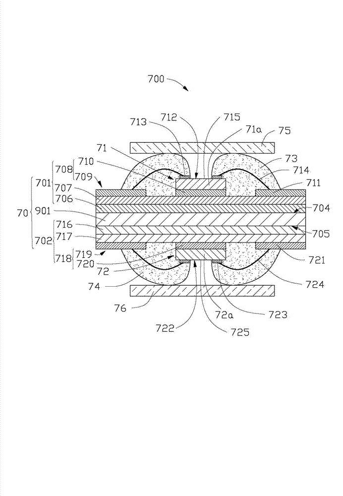
[0023] see Figure 1 to Figure 2 A double-sided circuit board structure 700 provided in the first embodiment of the present invention includes a circuit board 70, a first chipset 71, a second chipset 72, a first protective layer 73, a second protective layer 74, a first packaging glass 75 and the second packaging glass 76.

[0024] The circuit board 70 includes a spacer layer 901 , a first multilayer structure 701 and a second multilayer structure 702 . The spacer layer 901 includes a first surface 704 and a second surface 705 opposite to the first surface 704 . The first multilayer structure 701 is formed on the first side 704 , and the second multilayer structure 702 is formed on the second side 705 .

[0025] The first multilayer structure 701 includes a first circuit layer 706 formed on the first surface 704, a first intermediate layer 707 formed on the first circu...


PUM


Abstract

The invention relates to a double-sided circuit board structure which comprises a circuit board, a first chip group and a second chip group. The circuit board comprises a partition layer, a first multi-layer structure and a second multi-layer structure, the partition layer comprises a first surface and a second surface opposite to the first surface, the first multi-layer structure forms on the first surface, and the second multi-layer structure forms on the second surface. Each multi-layer structure comprises a first line layer, an intermediate layer and a second line layer, wherein the first line layer is formed on the first surface or the second surface, and the second line layer is formed on the intermediate layer which is formed on the first line layer and comprises a conductive line portion and a grounding portion. The first chip group is arranged on the grounding portion of the first multi-layer structure and electrically connected with the conductive line portion of the first multi-layer structure. The second chip group is arranged on the grounding portion of the second multi-layer structure and electrically connected with the conductive line portion of the second multi-layer structure.

Description

technical field [0001] The invention relates to a double-sided circuit board structure. Background technique [0002] At present, the development of computer technology requires the calculation / processing speed of electronic devices, the data transmission speed between electronic devices to be faster and faster, and / or the electronic devices to integrate more and more functions. Faster computing / processing speed, transmission speed and more functions will inevitably require electronic devices to integrate more electronic components. However, integrating more electronic components will increase the width of the circuit board carrying these electronic components, which is not in line with the current trend of miniaturization of electronic devices. Contents of the invention [0003] In view of this, it is necessary to provide a double-sided circuit board structure that can improve the integration of electronic components without increasing the width of the circuit board, so ...

Claims


Application Information

Patent Timeline
Patent Type & Authority Applications(China)
IPC IPC(8): H05K1/18H01L25/00H01L23/31H01L23/498
CPCH01L2224/8592H01L2924/181H01L2924/3011H01L2224/05553H01L2224/48091H01L2224/48227H01L2224/49175H01L2224/73265H01L2924/00014H01L2924/00H01L2924/00012
Inventor 吴开文
Owner HONG FU JIN PRECISION IND (SHENZHEN) CO LTD
Why Eureka
Try Eureka