Semiconductor device comprising junction type filed effect transistor and manufacturing method thereof

A technology of field effect transistors and semiconductors, applied in semiconductor/solid-state device manufacturing, semiconductor devices, transistors, etc., can solve problems such as reducing the pinch-off voltage of JFET

Active Publication Date: 2013-02-06
CHENGDU MONOLITHIC POWER SYST
View PDF6 Cites 13 Cited by
  • Summary
  • Abstract
  • Description
  • Claims
  • Application Information

AI Technical Summary

Problems solved by technology

[0005] In order to solve the problems described above, the present invention proposes an improved semiconductor device including a JFET and its manufacturing method, wherein the source region and the gate region of the JFET can maintain a sufficient distance, and the pinch-off voltage of the JFET can be reduced at the same time

Method used


Image

  • Semiconductor device comprising junction type filed effect transistor and manufacturing method thereof
  • Semiconductor device comprising junction type filed effect transistor and manufacturing method thereof
  • Semiconductor device comprising junction type filed effect transistor and manufacturing method thereof

Examples


Embodiment Construction

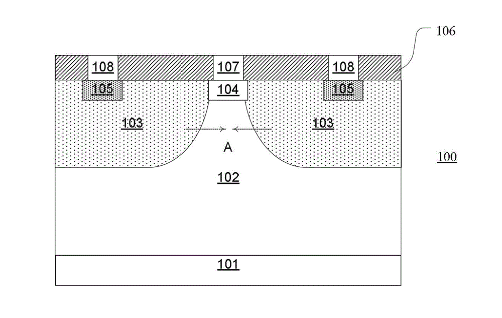
[0020] Exemplary embodiments of the present invention will be fully described below with reference to the accompanying drawings. In the various figures, the same elements are indicated with similar reference numerals. For clarity, various parts in the drawings are not drawn to scale, and detailed descriptions of some specific structures and functions are simplified. In addition, similar structures and functions that have been described in detail in some embodiments will not be repeated in other embodiments. Although terms of the present invention are described in conjunction with specific exemplary embodiments, these terms are applicable to any reasonable occasion in the art and should not be construed as being limited to the exemplary embodiments set forth herein.

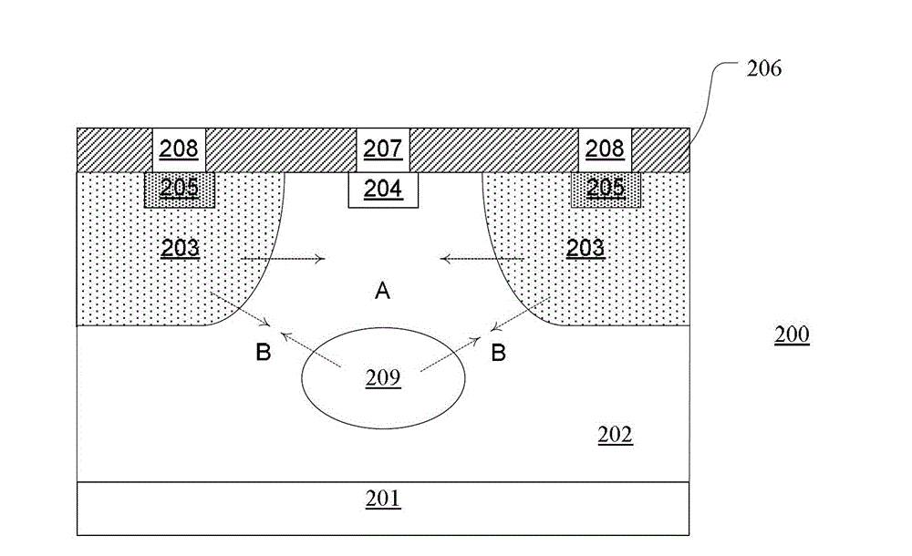
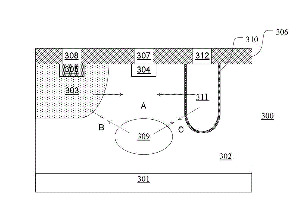
[0021] figure 2 is a cross-sectional view of a junction field effect transistor (JFET) 200 in accordance with one embodiment of the invention. exist figure 2 In, use with figure 1 Like reference numbers den...


PUM


Abstract

The invention discloses a semiconductor device comprising a junction type field effect transistor and a manufacturing method thereof. The semiconductor device comprises a junction type field effect transistor, wherein the junction type field effect transistor comprises a semiconductor underlay, an epitaxial layer, a body region, a source electrode region and a grid region, wherein the semiconductor underlay is provided with a first doping type and taken as a drain region of the junction type field effect transistor; the epitaxial layer is located on the semiconductor underlay and provided with a first doping type; the body region is located in the epitaxial layer and provided with a second doping type, and the types of the second doping type and the first doping type are reverse; the source electrode is located in the epitaxial layer and provided with a first doping type; and the grid region is located in the body region and provided with the second doping type, wherein the junction type field effect transistor further comprises a shielding layer, the shielding layer is provided with the second doping type, which is located in the epitaxial layer, and is also located in a conduction path between the source electrode region and the drain region. With the adoption of the shielding layer, a new pinch-off region is generated in the junction type field effect transistor, so as to reduce pinch-off voltage.

Description

technical field [0001] The present invention relates to a semiconductor device and a method of manufacturing the same, and more particularly to a semiconductor device including a junction field effect transistor and a method of manufacturing the same. Background technique [0002] figure 1 A cross-sectional view of a conventional N-channel junction field effect transistor (JFET) 100 is shown. The JFET 100 includes an N+ type drain region 101 (usually a substrate), an N-type epitaxial layer 102 located on the N+ type drain region 101, a P-type body region 103 located in the N-type epitaxial layer 102, and a P-type body region 103 located in the N+ type drain region 101. The N+ type source region 104 in the − type epitaxial layer 102 and between the P type body regions 103 , and the P+ type gate region 105 located in the P type body region 103 . The JFET 100 also includes an interlayer dielectric layer (ILDL) 106, a source contact 107 electrically connected to the N+ type so...

Claims


Application Information

Patent Timeline
Patent Type & Authority Applications(China)
IPC IPC(8): H01L29/78H01L29/10H01L21/336
CPCH01L27/0617H01L27/085H01L29/0619H01L29/0623H01L29/0653H01L29/1066H01L29/1608H01L29/24H01L29/407H01L29/41766H01L29/66712H01L29/66734H01L29/66909H01L29/7802H01L29/7803H01L29/7811H01L29/7813H01L29/7828H01L29/7832H01L29/8083H01L27/098H01L27/14679
Inventor 马荣耀李铁生张磊傅达平
Owner CHENGDU MONOLITHIC POWER SYST
Why Eureka
Try Eureka