


Quick Research
Generate reliable direction feasibility study reports for your R&D in just a few steps.

Technical Q&A
Discover and master advanced knowledge NOW. Basics, ideas, possibilities, all at once.

Find Solutions
As an expert in R&D theories, this can generate solutions to your technical problems instantly.

Evaluate Feasibility
Analyze your overall solution with one click, know your potential R&D risks in advance.

Monitor Landscape
Get weekly tech updates, stay abreast of the latest tech innovations and key insights.
LED integrated light source substrate and manufacturing method thereof
A light source substrate and substrate technology, applied in electrical components, circuits, semiconductor devices, etc., can solve the problems of not greatly improving LED light efficiency, reducing reliability and service life, increasing production costs, etc., to improve brightness and reliability. performance, low cost
- Summary
- Abstract
- Description
- Claims
- Application Information
AI Technical Summary
Problems solved by technology
Method used
Image

Examples
Embodiment Construction
[0022] The present invention will be further described below in conjunction with accompanying drawing and specific embodiment:
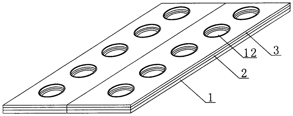
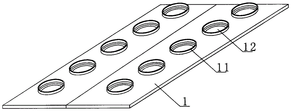
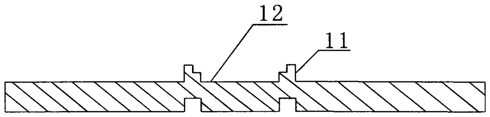
[0023] As shown in the figure, it includes a PCB circuit layer 3, a lamination layer 2 and a base layer 1, the lamination layer 2 is above the base layer 1, and the PCB circuit layer 1 is above the lamination layer 2, wherein: the base layer 1 is punched out The reflective cup body 12, the reflective cup body 12 uses a mold to recoil upward from the back to form a cup edge 11.
[0024] Preferably, the height of the cup edge 11 is equal to the thickness of the circuit layer 3 and the press-laminated layer 2 .
[0025] Preferably, the lamination layer 2 and the PCB circuit layer 3 are punched with holes corresponding to the cup edge 11 protruding from the substrate.
[0026] Preferably, the pressing layer 2 is generally a high-temperature hot-melt adhesive or a high-temperature double-sided adhesive,
[0027] A method for manufacturing an LED integra...
PUM
 Abstract
Description
Claims
Application Information
 - R&D Engineer
- R&D Manager
- IP Professional
- Industry Leading Data Capabilities
- Powerful AI technology
- Patent DNA Extraction
Browse by: Latest US Patents, China's latest patents, Technical Efficacy Thesaurus, Application Domain, Technology Topic, Popular Technical Reports.
© 2024 PatSnap. All rights reserved.Legal|Privacy policy|Modern Slavery Act Transparency Statement|Sitemap|About US| Contact US: help@patsnap.com