A method of fabricating LED vertical chips using wafer-level Si pattern substrates
A graphics substrate, wafer-level technology, used in semiconductor/solid-state device manufacturing, electrical components, circuits, etc., can solve the problems of chip processing changes, Si light absorption, etc., achieve good compatibility, simplify processes, and solve Si light absorption effect of the problem
- Summary
- Abstract
- Description
- Claims
- Application Information
AI Technical Summary
Problems solved by technology
Method used
Image
Examples
Embodiment 1
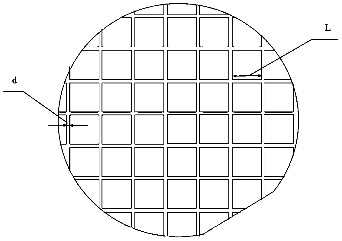
[0041] Such asfigure 1 As shown, a method of using a wafer-level Si pattern substrate to make an LED vertical chip in this embodiment includes the following steps:
[0042] 1) The making of Si pattern substrate: Adopt conventional gluing, exposure, etching process to realize the transfer of pattern on Si substrate, obtain Si pattern substrate; The pattern on described Si pattern substrate includes several matrixes Arranged square bumps, grooves are arranged between every two adjacent square bumps; the side length L=1mm of the square bumps, the width d=15 μm of the grooves, and the depth h=5 μm of the grooves ; The layout of the graphics is as follows image 3 shown.
[0043] 2) Growth of LED epitaxial layer: Si pattern substrate was cleaned by HF ultrasonic for 3min, N 2 After drying, the LED epitaxial layer is grown on the Si pattern substrate by thin film deposition method; the LED epitaxial layer includes AlN buffer layer, AlGaN step buffer layer, n-GaN layer, light emitt...
Embodiment 2
[0054] Except for the following features, this embodiment has the same or similar characteristics as Embodiment 1.
[0055] In step 1), the side length of the square bump on the Si substrate is L=0.5 mm, the groove width d=10 μm, and the groove depth h=10 μm.
Embodiment 3
[0057] Except for the following features, this embodiment has the same or similar characteristics as Embodiment 1.
[0058] The growth of the LED epitaxial layer in step 2) adopts the combination of metal-organic chemical vapor deposition and molecular beam epitaxy, and grows the LED epitaxial layer on the Si pattern substrate. The epitaxial layer includes an AlN buffer layer, an AlGaN step buffer layer, and an n-GaN layer. , a light emitting layer and a p-GaN layer.
PUM
| Property | Measurement | Unit |
|---|---|---|
| thickness | aaaaa | aaaaa |
| thickness | aaaaa | aaaaa |
| thickness | aaaaa | aaaaa |
Abstract
Description
Claims
Application Information
 - R&D
- Intellectual Property
- Life Sciences
- Materials
- Tech Scout
- Unparalleled Data Quality
- Higher Quality Content
- 60% Fewer Hallucinations
Browse by: Latest US Patents, China's latest patents, Technical Efficacy Thesaurus, Application Domain, Technology Topic, Popular Technical Reports.
© 2025 PatSnap. All rights reserved.Legal|Privacy policy|Modern Slavery Act Transparency Statement|Sitemap|About US| Contact US: help@patsnap.com


