


Quick Research
Generate reliable direction feasibility study reports for your R&D in just a few steps.

Technical Q&A
Discover and master advanced knowledge NOW. Basics, ideas, possibilities, all at once.

Find Solutions
As an expert in R&D theories, this can generate solutions to your technical problems instantly.

Evaluate Feasibility
Analyze your overall solution with one click, know your potential R&D risks in advance.

Monitor Landscape
Get weekly tech updates, stay abreast of the latest tech innovations and key insights.
Micro-nano pyramidal silicon/ingan hybrid pn junction solar cell and its preparation method
A technology of micro-nano pyramids and solar cells, which is applied in circuits, photovoltaic power generation, electrical components, etc., can solve the problems of reducing photogenerated current, reducing open circuit voltage, and increasing series resistance of devices, so as to enhance light absorption capacity, improve efficiency, and solve current problems. The effect of transmission
- Summary
- Abstract
- Description
- Claims
- Application Information
AI Technical Summary
Problems solved by technology
Method used
Image

Examples
Embodiment 1
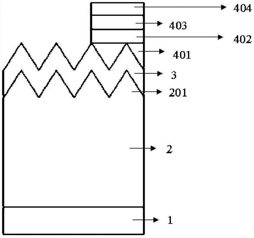
[0029]A p-electrode layer 1, the p-electrode layer is an Au material, which is manufactured on the opposite side of the p-Si layer by thermal evaporation coating; it grows in a low vacuum (10E5~10E2Pa) environment, and the growth temperature is controlled at 2000°C, the growth time is 30min, and the thickness is 80nm.
[0030] A p-type Si layer 2, the p-Si layer is made on the P electrode layer 1, and the p-Si is single-sided polished, the crystal orientation is (100), and its size is 10.0mm×10.5mm (±0.2mm) , the thickness is 520±10um, the crystal orientation is ±0.5, and the resistivity is 0.1Ω·cm. Its surface is corroded by KOH alkaline mixed solution for 20 minutes at room temperature to form a micro-nano pyramid structure, and the depth of the pyramid is 4um. as follows figure 1 Shown is a p-type Si layer with a micro-nano pyramid structure 201 grown on the P-electrode layer. The KOH alkaline mixed solution in the example is formed by mixing KOH with a mass concentratio...
Embodiment 2
[0035] A p-electrode layer 1, the p-electrode layer is an Au material, which is manufactured on the opposite side of the p-Si layer by thermal evaporation coating; it grows in a low vacuum (10E5~10E2Pa) environment, and the growth temperature is controlled at 3000°C, the growth time is 50min, and the thickness is 100nm.
[0036] A p-type Si layer 2, the p-Si layer is made on the P electrode layer 1, and the p-Si is single-sided polished, the crystal orientation is (100), and its size is 10.0mm×10.5mm (±0.2mm) , the thickness is 520±10um, the crystal orientation is ±0.5, and the resistivity is 0.5Ω·cm. Its surface is corroded by KOH alkaline mixed solution for 20 minutes at room temperature to form a micro-nano pyramid structure, and the depth of the pyramid is 5um. as follows figure 1 Shown is a p-type Si layer with a micro-nano pyramid structure 201 grown on the P-electrode layer. The KOH alkaline mixed solution in the example is formed by mixing KOH with a mass concentrat...
Embodiment approach 2
[0041] Example 1
[0042] A P-electrode layer 1, the P-electrode layer is made of Au material, which is fabricated on the opposite side of the p-Si layer by thermal evaporation coating; it grows in a low-vacuum environment, and the growth temperature is controlled to be 2000°C, and the growth time is It is 30min-50min, and the thickness is 80nm.
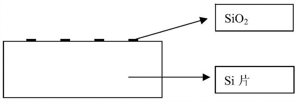
[0043] A p-type Si layer 2, the p-Si layer is made on the P electrode layer 1, and the p-Si is single-sided polished, the crystal orientation is (100), and its size is 10.0mm×10.5mm (±0.2mm) , the thickness is 520±10um, the crystal orientation is ±0.5, and the resistivity is 0.1Ω·cm. Its surface forms a micro-nano pyramid structure after processes such as photolithography and reactive ion etching, and the depth of the pyramid is 4um. The operation process is first to thermally oxidize the surface of the Si wafer to form a silicon dioxide layer with a thickness of about 5um, as shown in the figure Figure 2a shown. Then the photol...
PUM
 Abstract
Description
Claims
Application Information
 - R&D Engineer
- R&D Manager
- IP Professional
- Industry Leading Data Capabilities
- Powerful AI technology
- Patent DNA Extraction
Browse by: Latest US Patents, China's latest patents, Technical Efficacy Thesaurus, Application Domain, Technology Topic, Popular Technical Reports.
© 2024 PatSnap. All rights reserved.Legal|Privacy policy|Modern Slavery Act Transparency Statement|Sitemap|About US| Contact US: help@patsnap.com