High-resolution biosensor
A biosensor and high-resolution technology, applied in the field of sensors, can solve the problems of insufficient accuracy, high cost, single-base resolution nano-electrode integration, etc., and achieve the effect of avoiding pollution, simple method, and rapid gene electronic sequencing
- Summary
- Abstract
- Description
- Claims
- Application Information
AI Technical Summary
Problems solved by technology
Method used
Image
Examples
Embodiment 1
[0022] Embodiment 1: Preparation of nano functional layer unit
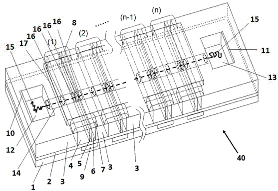
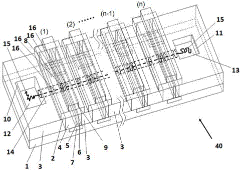
[0023] Such as Figure 5 Shown: (a) Single-layer graphene was transferred onto insulating boron nitride (20 nm), and then an insulating PMMA (polymethyl methacrylate) layer (500 nm) was spin-coated on top of the graphene. (b) Fabrication of nanopores (2 nm) by electron beam etching and etching.
[0024] Effect and analysis: In this embodiment, the first insulating layer uses boron nitride, and the second insulating layer uses polymer PMMA, but in the actual sensor, the first insulating layer and the second insulating layer can also use other insulating materials , such as SiO 2 , Al 2 o 3 , SiN x , BN, SiC, fluorinated graphene, polyvinyl alcohol, poly(4-vinylphenol), polymethylmethacrylate, or divinyltetramethyldisiloxane-bis(benzocyclobutene) A mixture of one or more of them. For the nano-functional layer, not only single-layer graphene can be used, but also double-layer or multi-layer graphene can be us...
Embodiment 2
[0026] Embodiment 2: Preparation of Field Effect Transistor Unit
[0027] Such as Figure 6 Shown: (a) 30 nm thick HfO was prepared on a Si (500 μm) substrate by atomic layer deposition 2 As a dielectric layer for field effect transistors. (b) Transfer of the as-prepared sandwich-like structure to Si (500 μm) / HfO 2 (30 nm). (c) Ti (2 nm) / Au (50 nm) was prepared on a sandwich-like structure by photolithography and etching techniques as the source and drain electrodes of field effect transistors.
[0028] Effect and analysis: In this embodiment, Si with a thickness of 500 μm is used as the substrate, and Si with other thicknesses or other materials such as GaN, Ge, GaAs, SiC, and Al can also be used 2 o 3 , SiN x , SiO 2 , HfO 2 , polyvinyl alcohol, poly(4-vinylphenol), divinyltetramethyldisiloxane-di(benzocyclobutene) or polymethylmethacrylate or a mixture of one or more.
[0029] For the dielectric layer, this example uses HfO 2 , but other dielectric materials such...
Embodiment 3
[0032] Example 3: Preparation of micro-nanofluidic device unit
[0033] Such as Figure 7 Shown: 300 nm SiO grown by thermal oxidation on a 500 μm thick silicon substrate 2 layer; then using photolithography and etching techniques on SiO 2 The first storage chamber (2 mm × 2 mm), the second storage chamber (2 mm × 2 mm) and the micro-nano separation channel (aperture: 200 nm) were prepared in the first layer; finally, the Pt (30 nm) layer as the first electrophoretic electrode and the second electrophoretic electrode.
[0034] Effect and analysis: this example uses Si / SiO 2 To prepare micro-nanofluidic devices, in actual biosensors, the integration of material functions with field-effect transistors can be considered, and different materials can be selectively used. The size and shape of the first and second storage chambers can be determined according to actual conditions; other conductive materials can be used for the first and second electrophoretic electrodes.
PUM
 Abstract
Description
Claims
Application Information


