

Surface plasma resonance sensing chip and preparation method thereof and application thereof
A surface plasmon and sensor chip technology, applied in ion implantation plating, coating, instrumentation, etc.
- Summary
- Abstract
- Description
- Claims
- Application Information
AI Technical Summary
Problems solved by technology
Method used
Image

Examples
Embodiment 1
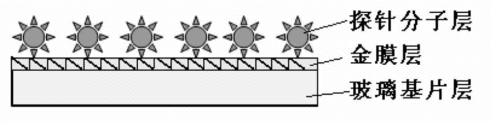
[0069] A surface plasmon resonance sensing chip, comprising a glass substrate layer, a gold film layer, and a probe molecule layer; a gold film layer is arranged on the glass substrate layer, and a probe molecule layer is arranged on the gold film layer; the gold film layer The thickness of the probe molecule layer is 10-60nm; the thickness of the probe molecule layer is 1-100nm; the probe molecule layer is a layer of one or two or more probe molecules in the following structures:
[0070]
[0071] In the formula, Ar 1 Thiophene, pyrrole, benzene, naphthalene, anthracene, pyrene, indole, coumarin, fluorescein, carbazole, rhodamine, cyano dyes, fluorene or quinoline, respectively;
[0072] Ar 2 One of the following structures respectively:
[0073]
[0074] X, Y, W are O, S, N-R respectively 5 or Si-R 6 R 7 ;
[0075] Z 1 ,Z 2 , R 1 , R 2 , R 3 , R 4 , R 5 , R 6 , R 7 , R 8 , R 9 , R 10 , R 11 , R 12 , R 13 , R 14 , R 15 Hydrogen atom; 1-18 carbon a...
Embodiment 2
[0079] A method for preparing a surface plasmon resonance sensor chip, the specific steps are:
[0080] 1) Using vacuum evaporation technology, a thickness of 50nm gold is plated on the surface of the glass substrate;
[0081] 2) The glass substrate coated with the gold film obtained in step 1) is completely immersed in the probe molecule (PT1) solution with a concentration of 0.01mg / mL, and the solvent is N,N-dimethylformamide, Place at room temperature for 1 hour;
[0082] 3) After soaking completely, take out the glass substrate, rinse the glass substrate repeatedly with double distilled water to obtain a chip, and store it in double distilled water for later use.
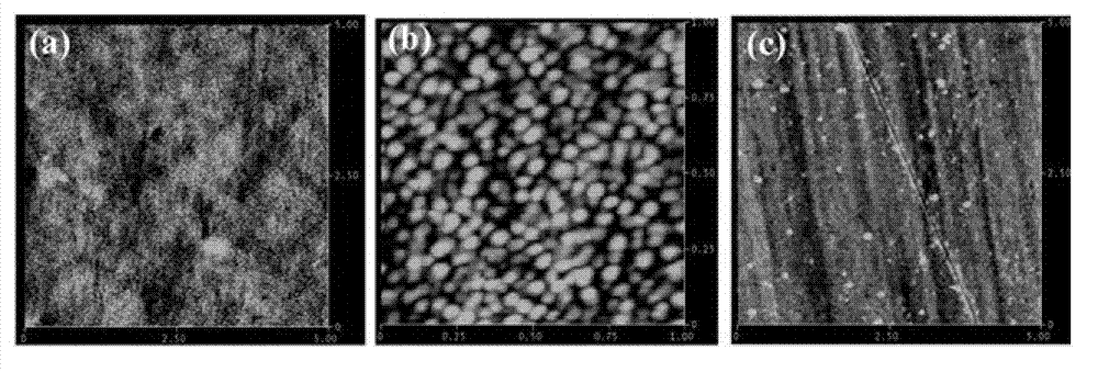
[0083] figure 2 An atomic force microscope (AFM) image of a gold film coated on a glass substrate. (a) Gold film surface, 5um range; (b) Gold film surface, 1um range. figure 2 The white particles in (C) are probe molecules, and their coverage is about 20%.
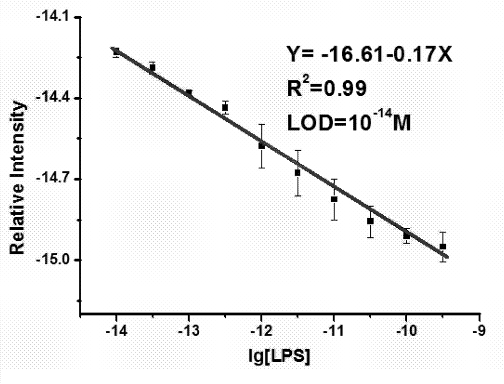
[0084] The surface plasmon resonance sensor chi...
Embodiment 3
[0087] A method for preparing a surface plasmon resonance sensor chip, the specific steps are:
[0088] 1) Using magnetron sputtering technology, the thickness of 50nm gold is plated on the surface of the glass substrate;
[0089]2) The glass substrate plated with gold film obtained in step 1) is completely immersed in the probe molecule (PT1) solution with a concentration of 10 mg / mL, the solvent is acetonitrile, and placed at room temperature for 10 hours;
[0090] 3) After soaking completely, take out the glass substrate, rinse the glass substrate repeatedly with double distilled water to obtain a chip, and store it in double distilled water for later use.
PUM
| Property | Measurement | Unit |
|---|---|---|
| thickness | aaaaa | aaaaa |
| thickness | aaaaa | aaaaa |
| concentration | aaaaa | aaaaa |
Abstract
Description
Claims
Application Information