Supercharge Your Innovation With Domain-Expert AI Agents!

Semiconductor package structure with low inductance

A semiconductor and metal conductor technology, applied in semiconductor devices, semiconductor/solid-state device manufacturing, semiconductor/solid-state device components, etc., can solve the problems of unable to provide high-speed synchronous switching output noise, not very effective, increasing substrate size, etc. , to achieve a stable common ground reference, increase the available space, and reduce the effect of inductance

Active Publication Date: 2013-02-13
NAN YA TECH
View PDF3 Cites 2 Cited by
  • Summary
  • Abstract
  • Description
  • Claims
  • Application Information

AI Technical Summary

Problems solved by technology

[0005] One way to reduce the above inductance is to increase the thickness of the bond wires, but this is not very effective because the number of bond wires that can be used is limited by the space available in the package
Most of today's package designs have a crowded routing environment. In addition, using thicker bonding wires will involve increasing the size of the substrate. That is to say, it cannot provide an effective solution to reduce the output noise of high-speed synchronous switching.

Method used


Image

  • Semiconductor package structure with low inductance
  • Semiconductor package structure with low inductance
  • Semiconductor package structure with low inductance

Examples


Embodiment Construction

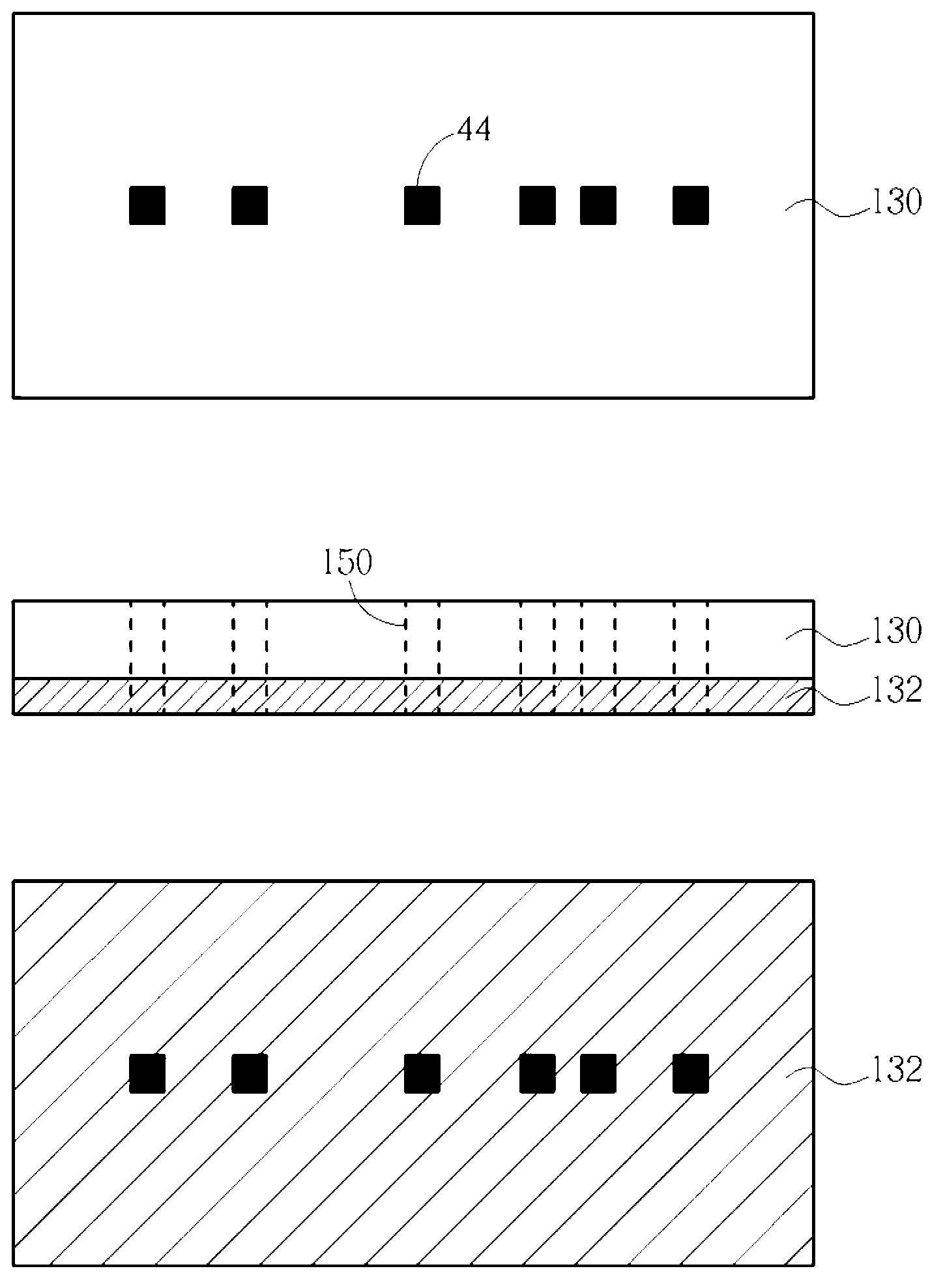
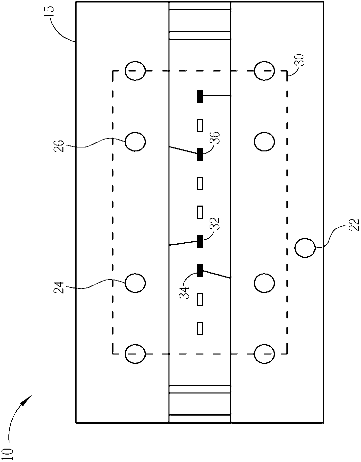
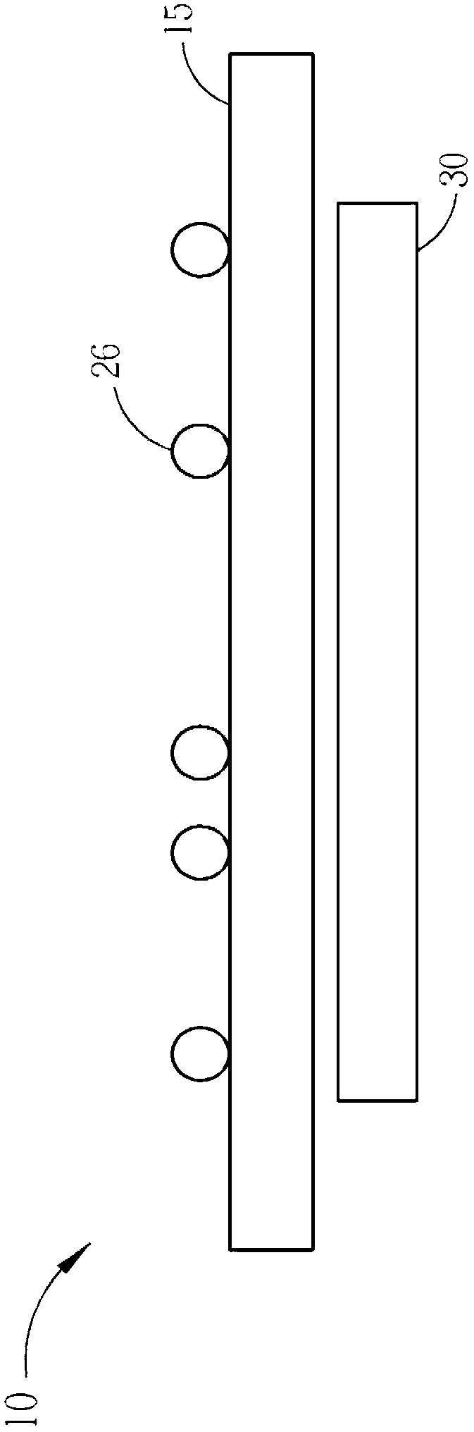
[0029] Therefore, one of the objectives of the present invention is to provide a semiconductor package structure with reduced inductance while still maintaining a small-sized substrate. Several embodiments for realizing the object of the present invention will be described in detail as follows.

[0030] In the embodiments provided by the present invention, the inductance of the ground power supply rail (indicated by VSSQ) is reduced as a reference for description. The method used to reduce the inductance of the ground supply rail VSSQ involves establishing a common ground reference point that eliminates the need for an isolated ground point or multiple ground points. (ground point) needs. Since the ground is always the same, it is practical to use a common ground reference while still allowing for different magnitudes of the supply VCC / VDDQ, that is, when the current demand changes, the Different power balls are used as the power rail VDDQ, while the ground power rail VSSQ i...


PUM


Abstract

A semiconductor package structure includes: a substrate comprising a plurality of power supply balls on a first surface of the substrate, a first metal conductor on a second surface of the substrate and at least one via coupling a power supply ball to the first metal conductor of the substrate; a die, comprising a plurality of bond pads on a first surface of the die, a first metal conductor on a second surface of the die and at least one via coupling a bond pad to the first metal conductor of the die; and a plurality of first wire bonds for coupling the first metal conductor of the substrate to the first metal conductor of the die.

Description

technical field [0001] The present invention relates to semiconductor packaging, and more particularly to semiconductor packaging structures with low power supply inductance. Background technique [0002] In modern computers and electronic products, the use of memory is quite common, such as dynamic random access memory (Dynamic Random Access Memory, DRAM) and logic components (Logic device), and these memory components are usually packaged (packaged) For a semiconductor chip (chip). For example, a packaging example of DRAM is formed by placing the die of semiconductor DRAM under a single layer substrate, and this method is often called Board-on-Chip (BOC) design. One side of the die contains bond pads and can be considered a circuit side, while the substrate also has a circuit side which contains power supply soldering balls of the type Multiple internal conductive traces (conductive trace) and multiple external contact points (contact). DRAM packaging is accomplished b...

Claims


Application Information

Patent Timeline
Patent Type & Authority Applications(China)
IPC IPC(8): H01L23/50H01L27/108H01L21/48H01L21/8242
CPCH01L23/13H01L2924/15311H01L23/498H01L2224/4824H01L23/147H01L2224/49175H01L2224/4918H01L24/49H01L2224/48091H01L2224/4903H01L2224/48227H01L2924/30107H01L24/48H01L23/49827H01L2924/00014H01L2924/00H01L2224/45099H01L2224/05599
Inventor 亚伦·威利马炎涛
Owner NAN YA TECH
Features
  • R&D
  • Intellectual Property
  • Life Sciences
  • Materials
  • Tech Scout
  • Unparalleled Data Quality
  • Higher Quality Content
  • 60% Fewer Hallucinations
Learn More