Debugging method for large-scale field programmable gate array (FPGA) design

A debugging method and large-scale technology, applied in the direction of measuring devices, instruments, measuring electronics, etc., can solve the problems of long signal time, limited data acquisition and storage depth, waste of time and cost, etc.

Active Publication Date: 2013-03-06
BEIJING CEC HUADA ELECTRONIC DESIGN CO LTD
View PDF7 Cites 4 Cited by
  • Summary
  • Abstract
  • Description
  • Claims
  • Application Information

AI Technical Summary

Problems solved by technology

[0004] Some methods require re-routing the FPGA layout, which will cause a huge waste of time and cost
[0005] Some methods need to use the BRAM resources inside the FPGA, and the data acquisition and storage depth is limited. In the debugging of large-scale FPGA design, sometimes the signal time to be observed is longer. This type of method also has its limitations.
[0006] There are also some methods that can realize the test of multiple internal signals to be tested on one pin, but the grouping needs to be set in advance, and the selection of any internal signal to be tested by one pin cannot be realized. In addition, the software of each manufacturer needs to cooperate. Testing is more expensive

Method used


Image

  • Debugging method for large-scale field programmable gate array (FPGA) design
  • Debugging method for large-scale field programmable gate array (FPGA) design

Examples


Embodiment Construction

[0015] The present invention will be described in detail below with reference to the accompanying drawings.

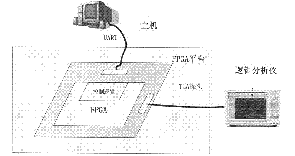
[0016] The invention provides a debugging method suitable for large-scale FPGA design, the main purpose is to improve the debugging efficiency on the FPGA prototype, reduce the test cost, and realize the selection of an external test pin to any internal signal to be tested. The main principle is to operate the control logic inside the FPGA through the host UART interface to realize the connection between the internal signal to be tested and the external test pin.

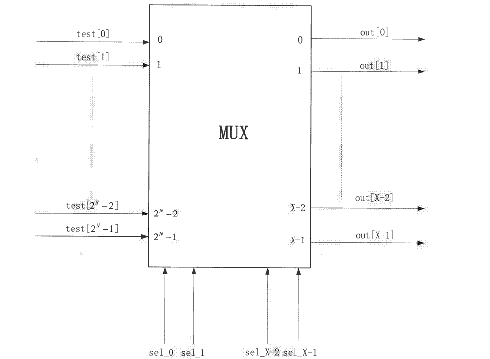
[0017] First, the internal signal to be tested needs to be set up in advance, assuming there are 2 N If you want to observe the signal, you need to set these 2 in advance in the design. N Each signal is set as the internal signal to be tested and connected to the control logic inside the FPGA.

[0018] Control logic input is 2 N The output is connected to the external test pins. Assuming that the number o...


PUM


Abstract

The invention provides a debugging method for large-scale field programmable gate array (FPGA) design, and mainly aims to provide a relatively general debugging method. By the debugging method, the time of debugging an FPGA prototype is saved, and the efficiency of debugging the FPGA prototype is improved. The main theory is that a redundant control logic is designed; and a main machine end configures a corresponding register of the control logic through operation of a universal asynchronous receiver / transmitter (UART), so that an external test pin is selectively connected to a signal to be tested in a certain FPGA chip. By the method, the structure is simple; the method is easy to implement; the external test pin can test a plurality of inner signals to be tested of the FPGA chips; and during test, the inner signals to be tested of certain FPGA chips can be freely selected, and the signals are not required to be grouped in advance.

Description

technical field [0001] The invention relates to the field of FPGA design, in particular to a debugging method in FPGA design. Background technique [0002] In recent years, as the scale of FPGA design has become larger and larger, the scale of FPGA chips has also become larger and larger, and the impact of debugging on FPGA prototypes on project progress has become critical. For example, in a wireless LAN FPGA design, debugging occupies a large proportion, so accelerating the debugging on the FPGA prototype can effectively improve the project schedule. [0003] Now, with regard to debugging on FPGA prototypes, there are also some common debugging tools and methods on the market, such as directly modifying the code to assign the required signals to external test pins, embedded logic analyzers, and FPGA Editor to lead internal signals to internal signals. to external test pins, dynamic probes from Agilent, etc. [0004] Some methods need to perform FPGA layout and routing ag...

Claims


Application Information

Patent Timeline
IPC IPC(8): G01R31/3177
Inventor 龚永鑫
Owner BEIJING CEC HUADA ELECTRONIC DESIGN CO LTD
Why Eureka
Try Eureka