Wiring method of FPGA prototype verification system

A prototype verification and wiring method technology, applied in the field of FPGA prototype verification system wiring, can solve problems such as signal delay increase, FPGA prototype system performance degradation, and large delay ratio.

Pending Publication Date: 2021-09-14
NANJING NORMAL UNIVERSITY
View PDF0 Cites 2 Cited by
  • Summary
  • Abstract
  • Description
  • Claims
  • Application Information

AI Technical Summary

Problems solved by technology

[0005] Although TDM technology increases the number of signal transmissions between FPGAs, it also has negative effects, the most important of which is the increase in signal delay
This type of delay accounts

Method used


Image

  • Wiring method of FPGA prototype verification system
  • Wiring method of FPGA prototype verification system
  • Wiring method of FPGA prototype verification system

Examples


Embodiment Construction

[0046] The present invention will be described in further detail below in conjunction with the accompanying drawings.

[0047] Table 1 is the common parameter meaning of the present invention:

[0048] Table 1 parameter description

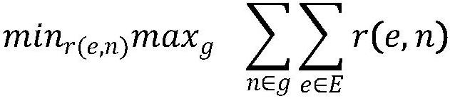
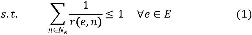
[0049] symbol meaning G A collection of all groups g group N A collection of all the nets n net E A collection of all connections between FPGAs e Connection between FPGAs V A collection of all FPGAs v Single FPGA r(e, n) Time division multiplexing ratio allocated when network n uses edge e

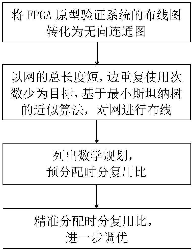
[0050] The present invention proposes a wiring method of FPGA prototype verification system, such as figure 1 As shown, it specifically includes the following steps:

[0051] Step 1: Convert the wiring diagram of the FPGA prototype system into an undirected connected graph.

[0052] Transform the wiring diagram of the FPGA prototype system into an undirected connected graph G(V, E), reco...


PUM


Abstract

The invention discloses a wiring method of an FPGA prototype verification system. The wiring method comprises the following steps: converting a wiring diagram of the FPGA prototype system into an undirected connected diagram; taking the short total length of the network and the small number of times of repeated use of edges as targets, and performing wiring on the network based on an approximation algorithm of a minimum Steiner tree; according to the wiring condition and the constraint condition of the network, listing a mathematical plan, and pre-allocating a time division multiplexing ratio; accurately distributing the time division multiplexing ratio, and carrying out further tuning. According to the method, the FPGA prototype system can be successfully wired, and the group with the largest negative effect in all the groups is minimized, so that the system delay is greatly reduced, and the performance of the whole FPGA system is improved.

Description

technical field [0001] The invention belongs to the field of electronic design automation, and in particular relates to a wiring method for an FPGA prototype verification system. Background technique [0002] As the VLSI process becomes more and more advanced, if some loopholes are found in actual manufacturing, the cost of correcting the design and remanufacturing is huge, so it is very necessary to verify at each stage of the VLSI design process , and the cost and time required for verification occupies half of the chip design. [0003] Currently, there are three methods for performing chip logic verification, namely software simulation, processor-based hardware simulation accelerated software simulation, and FPGA prototype verification system. Among them, the verification method based on FPGA prototype has high execution speed, low cost and rich testing experience, so it has high application value. However, the capacity of a single FPGA is limited, so a Multi-FPGA proto...

Claims


Application Information

Patent Timeline
IPC IPC(8): G06F30/394G06F111/04
CPCG06F30/394G06F2111/04
Inventor 张晓岩郭龙坤杭毅成孙龙彭辉鸿戴国伟周洋李敏
Owner NANJING NORMAL UNIVERSITY
Why Eureka
Try Eureka