Display and electronic system

A display and light-emitting layer technology, applied in circuits, electrical components, electrical solid-state devices, etc., can solve the problems of reduced life, increased power consumption, and reduced light output, and achieve the effects of suppressing reflection, low power consumption, and long life

Active Publication Date: 2013-03-06
JOLED INC
View PDF6 Cites 17 Cited by
  • Summary
  • Abstract
  • Description
  • Claims
  • Application Information

AI Technical Summary

Problems solved by technology

As a result, light output is reduced, leading to increased power consumption due to increased current density and reduced lifetime

Method used


Image

  • Display and electronic system
  • Display and electronic system
  • Display and electronic system

Examples


no. 1 example

[0041] [Structure of Display 1]

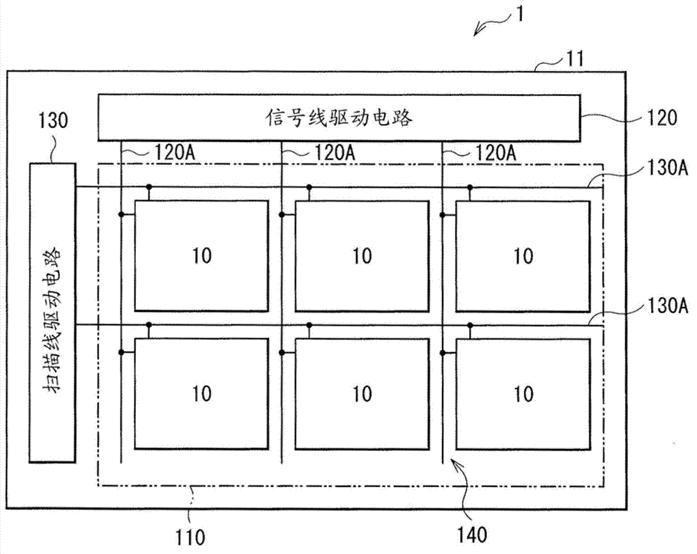
[0042] figure 1The configuration of the display (display 1 ) according to the first embodiment of the present invention is shown. The display 1 is an organic electroluminescence (EL) display in which a plurality of organic EL devices 10 emitting red, green and blue light, for example, are arranged in a matrix on a substrate 11 to define a display area 110 . A driving circuit 120 and a scanning line driving circuit 130 that drive signal lines are provided at the periphery of the display area 110 , and each of the signal line driving circuit 120 and the scanning line driving circuit 130 is provided for image display.

[0043] (overall structure)

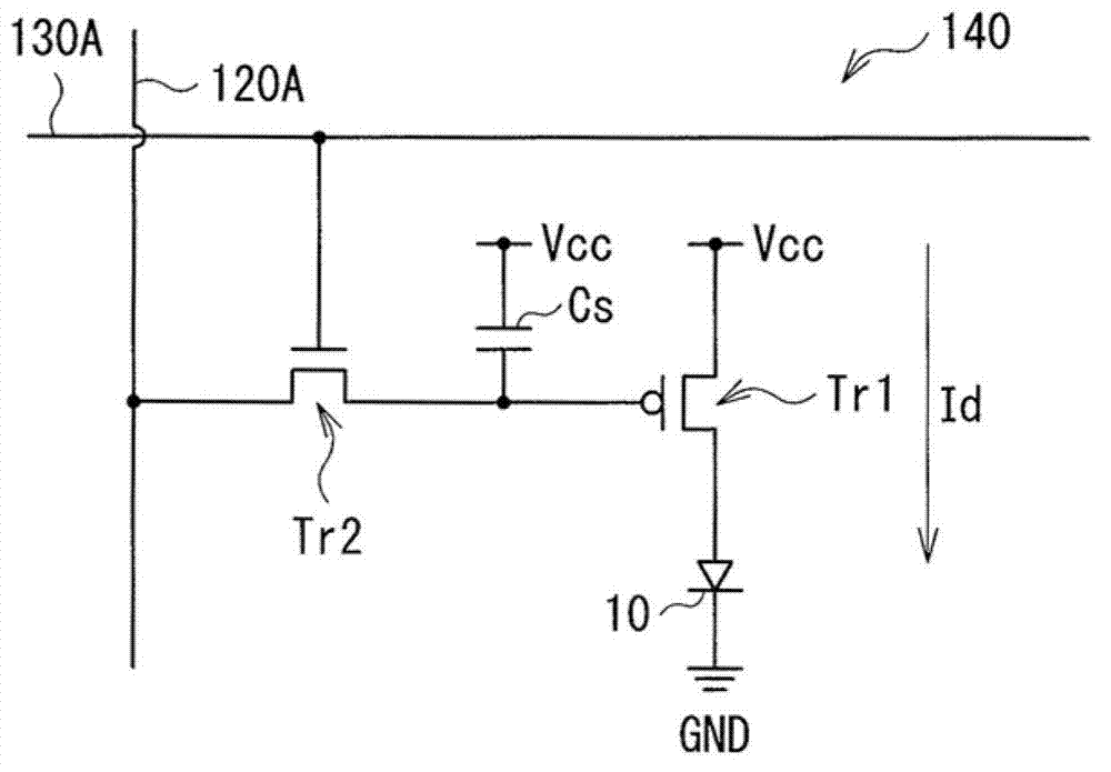
[0044] A plurality of pixel driving circuits 140 are provided in the display area 110 . figure 2 An exemplary pixel driver circuit 140 is shown. The pixel driving circuit 140 is an active driving circuit provided below the lower electrode 12 described later. Specifically, the pixel driving circui...

no. 2 example

[0150] The display (display 2 ) according to the second embodiment of the present invention differs from that of the first embodiment in that an external light reflection suppression layer 24 is provided between a quarter retardation film 25 and a reflective polarizer 26 . Other structures of the display 2 are similar to the display 1, and its functions and effects are also similar to the display 1.

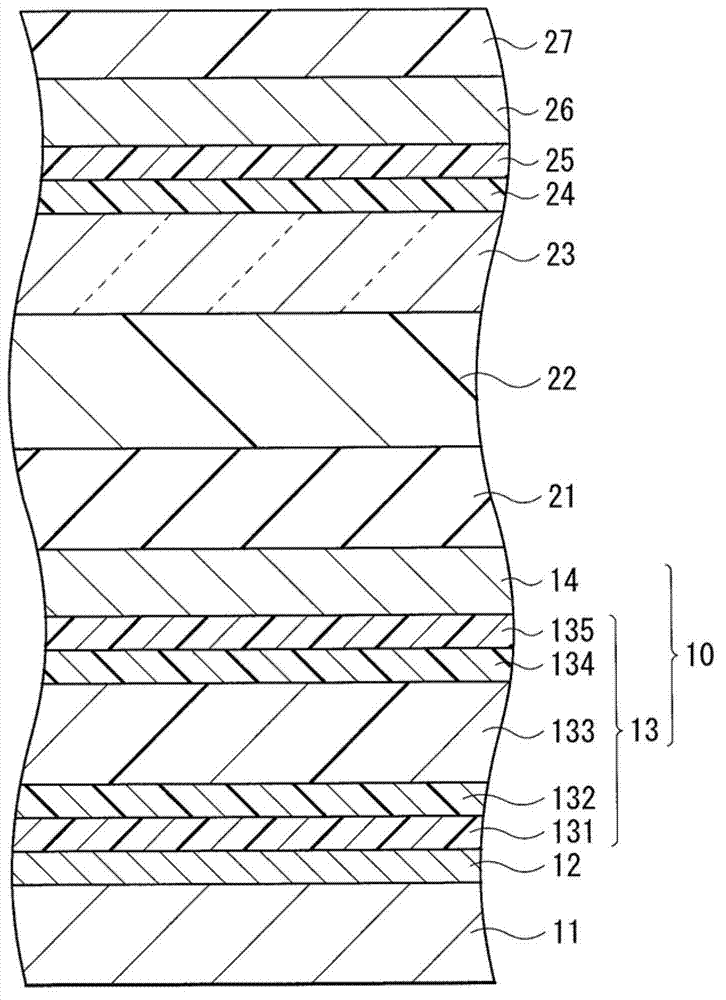
[0151] Figure 15 A cross-sectional configuration of a display 2 is shown in which the organic EL device 10 is sealed by a protective layer 21 , a sealing portion 22 and a counter substrate 23 as in the display 1 . Display 2 differs from display 1 in the configuration of the display surface side of counter substrate 23 in which quarter retardation film 25, external light reflection suppression layer 24, reflective polarizing plate 26, and absorbing polarizing plate 27 are sequentially provided.

[0152] (modules and application examples)

[0153] Application examples of each di...

application example 1)

[0157] Figure 17 The appearance of a television device to which the display according to the embodiment and the modification is applied is shown. The television device has, for example, an image display screen portion 300 including a front panel 310 and a color filter glass 320 . The image display screen section 300 is configured by the display according to the embodiment and the modification.


PUM


Abstract

A display includes: a light emitting layer; a reflective section reflecting light, that enters through the light emitting layer, to a display surface; an absorption-type polarizing plate provided on the display surface; a retardation film provided between the light emitting layer and the absorption-type polarizing plate; a reflection-type polarizing plate provided between the retardation film and the absorption-type polarizing plate, and reflecting, among light transmitted by the retardation film, light in a predetermined light-axis direction; and an outside-light reflection suppression layer provided between the light emitting layer and the reflection-type polarizing plate, and absorbing part of outside light.

Description

technical field [0001] The present invention relates to self-luminous displays, such as organic electroluminescent (EL) displays, and electronic systems including the displays. Background technique [0002] With the development of the information and communication industry, higher performance display devices are required. For example, each of an organic electroluminescence (EL) display, an inorganic EL display, and a field emission display (FED) is a display including a self-luminous display device, and has been favored due to its wide viewing angle, high contrast ratio, and high response speed. Think of it as the next generation of displays. For example, an organic EL device includes a lower electrode, a light-emitting layer, an upper electrode, and a counter substrate sequentially from the driving substrate, and is roughly divided into a bottom emission type and a top emission type. The display light of the bottom emission type is extracted through the driving substrate, ...

Claims


Application Information

Patent Timeline
Patent Type & Authority Applications(China)
IPC IPC(8): H01L27/32H01L51/54H01L51/52
CPCH01L2251/5315H01L51/5281H01L51/5218H10K50/818H10K50/86H10K2102/3026G02B5/30
Inventor 福田俊广
Owner JOLED INC
Why Eureka
Try Eureka