Universal debugging interface-based SoC (System on Chip) hardware debugger

A debugging interface and hardware debugging technology, which is applied in the detection of faulty computer hardware, function inspection, etc., can solve problems such as waste of resources, inability to unify, and slow debugging speed, and achieve the effect of improving performance

Inactive Publication Date: 2013-03-13
NO 771 INST OF NO 9 RES INST CHINA AEROSPACE SCI & TECH
View PDF3 Cites 21 Cited by
  • Summary
  • Abstract
  • Description
  • Claims
  • Application Information

AI Technical Summary

Problems solved by technology

[0009] Based on the above-mentioned mainstream hardware debugging modules in the industry, it can be known that the ARM debugging system uses the JTAG pin debugging in the SoC circuit for boundary scan and chip interconnection testing in order to unify the chip-level testing and chip-level debugging methods. Although the precious pin resources of the chip are saved, the ARM debugging system inserts the scan chain on the critical path of the processor, which has an "intrusive" impact on the system and limits the improvement and exertion of system performance.
The debugging support module DSU based on the UART serial port uses the serial port to transmit debugging information, and the debugging speed is slow. It needs five additional chip pins including uart_tx, uart_rx, DBGEN, DBGQER, and DBGREQ, but does not need to insert an additional scan connection, and because the 500 The use of 502 makes the debugging system have no "intrusive" influence on the performance of SoC. Its major defect is that the debugging of chip-level SoC can use the debugging support module DSU based on UART serial port, but due to the higher application level (such as Board-level, whole machine) can only be debugged through the IEEE standard JTAG interface, so the debugging support module DSU based on the UART serial port cannot unify the chip machine, board-level test and chip-level test methods. Different test versions are produced during the debugging phase, which greatly wastes resources

Method used


Image

  • Universal debugging interface-based SoC (System on Chip) hardware debugger
  • Universal debugging interface-based SoC (System on Chip) hardware debugger
  • Universal debugging interface-based SoC (System on Chip) hardware debugger

Examples


Embodiment Construction

[0048] The present invention will be described in further detail below in conjunction with the accompanying drawings, which are explanations rather than limitations of the present invention.

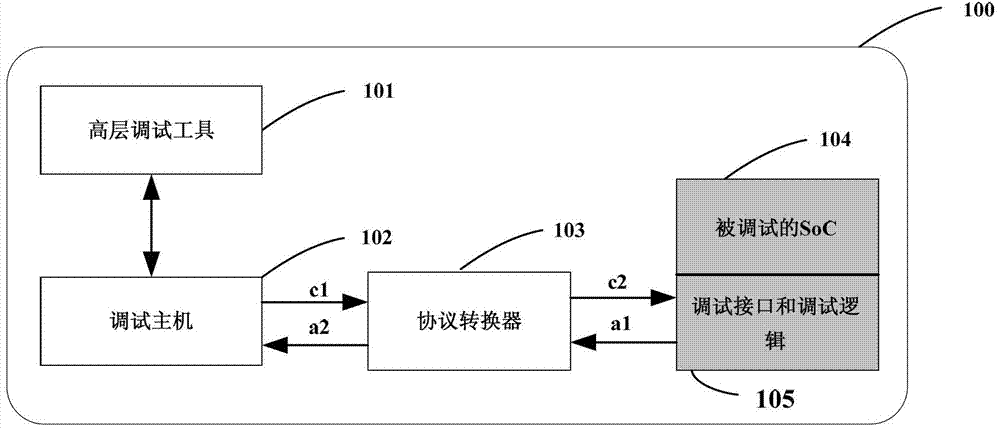
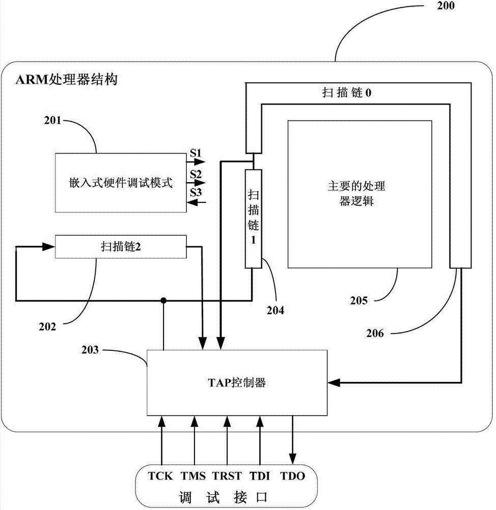
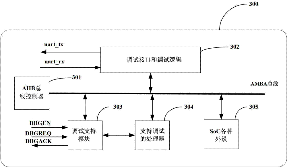
[0049] A SoC hardware debugger based on a general debugging interface, including a general debugging interface, a TAP controller, a scan chain, a debugging control register module, a synchronization module, a JTAG-AHB protocol conversion module, an AHB-DMA module, an AHB bus controller, a debugging Support modules, SoC peripheral modules, and debug-enabled processors;

[0050] The general debugging interface is connected to an external debugging device, and the debugging information is updated to the debugging control register module through the scan chain controlled by the TAP controller;

[0051] The debugging control register module sends the debugging information to the JTAG-AHB protocol conversion module through the synchronization module; the debugging control register module and t...


PUM


Abstract

The invention discloses a universal debugging interface-based SoC (System on Chip) hardware debugger, which comprises a universal debugging interface, a TAP controller, a scan chain, a debugging control register module, a synchronizing module, a JTAG-AHB (Joint Test Action Group-Advanced High-performance Bus) protocol conversion module, an AHB-DMA (Advanced High-performance Bus-Direct Memory Access) module, an AHB bus controller, a debug support unit (DSU), an SoC peripheral module and a processor for supporting debugging. According to the universal debugging interface-based SoC hardware debugger, a JTAG port is applied to the DSU of a GAISLER laboratory open source for the first time, the scan chain is prevented from being plugged into a key path of the processor, and the structure and the performance of the SoC hardware debugger are superior to those of the normal hardware debugging modules at present. The SoC hardware debugger has beenis subjected to tape-out verification to prove that the function is correct and reliable.

Description

Technical field: [0001] The invention belongs to the field of semiconductor integrated circuits and relates to a SoC hardware debugger based on a general debugging interface. Background technique: [0002] According to the resources used in the SoC (System on Chip) debugging process, SoC debugging can be divided into software debugging and hardware debugging. Software debugging is mainly to reside in the monitoring program in the running program, and its debugging function is relatively simple, which can no longer meet the actual engineering needs; the strategy of hardware debugging is to integrate related functional modules that support debugging in the SoC system. Operate these functional modules to quickly locate problems in the use of SoC circuits. Hardware debugging has become the mainstream of debugging technology in SoC engineering applications. [0003] A typical hardware-based debug system such as figure 1 Shown in 100. The high-level debugging tool 101 is a wind...

Claims


Application Information

Patent Timeline
Patent Type & Authority Applications(China)
IPC IPC(8): G06F11/26
Inventor 段青亚陈庆宇盛廷义赵恒星李剑
Owner NO 771 INST OF NO 9 RES INST CHINA AEROSPACE SCI & TECH
Why Eureka
Try Eureka