Modeling method for PSP mismatch model of MOS transistor

A technology of MOS transistor and mismatch model, which is applied in the fields of instrumentation, calculation, electrical and digital data processing, etc., can solve the problem of less research on MOSFET process fluctuation model, and achieve the effect of high accuracy and clear physical meaning.

Active Publication Date: 2013-03-13
EAST CHINA NORMAL UNIV +1
View PDF3 Cites 14 Cited by
  • Summary
  • Abstract
  • Description
  • Claims
  • Application Information

AI Technical Summary

Problems solved by technology

However, there are few researches on systematically establishing integrated circuit MOSFET process fluctuation models.

Method used


Image

  • Modeling method for PSP mismatch model of MOS transistor
  • Modeling method for PSP mismatch model of MOS transistor
  • Modeling method for PSP mismatch model of MOS transistor

Examples


Embodiment Construction

[0038] The present invention will be further elaborated below in conjunction with the accompanying drawings and examples. The following examples do not limit the present invention. Without departing from the spirit and scope of the inventive concept, changes and advantages that can be imagined by those skilled in the art are all included in the present invention.

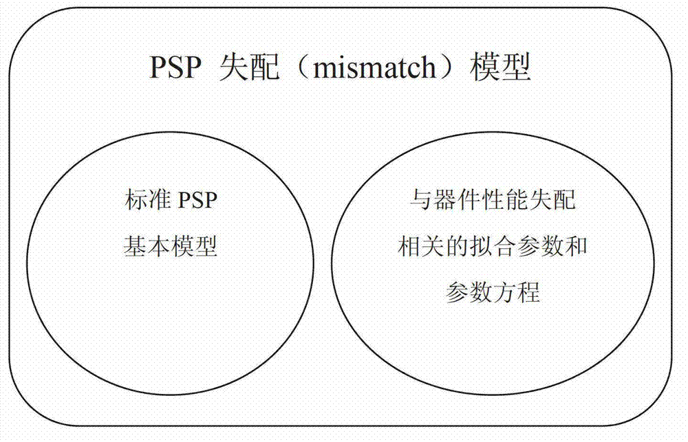
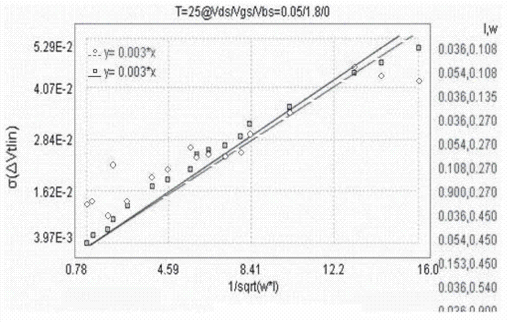
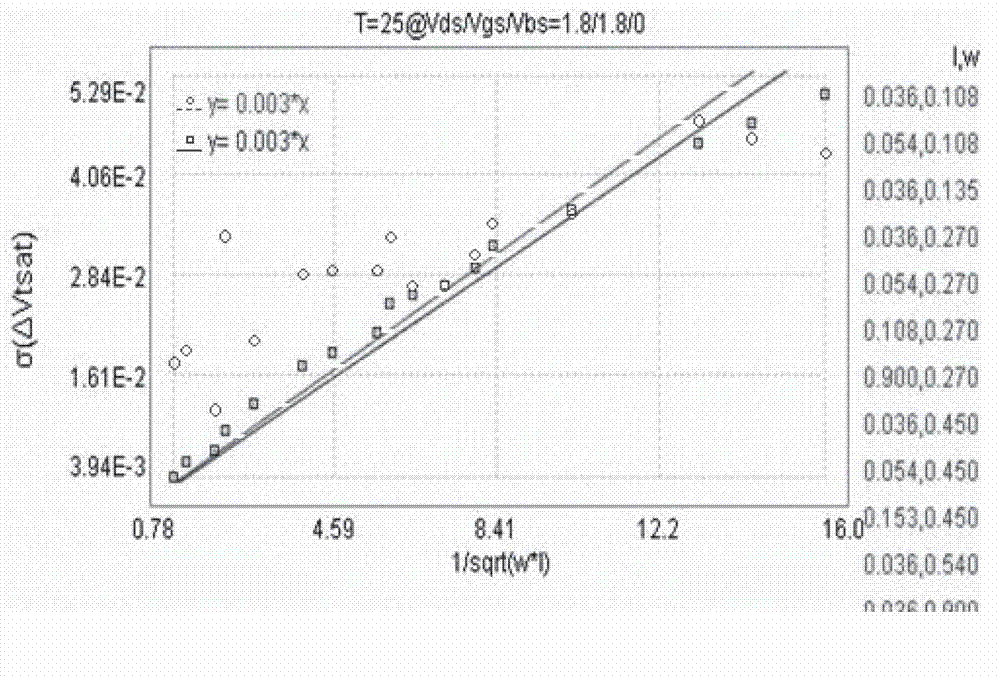
[0039] The invention provides a modeling method of a PSP mismatch model of a MOS transistor, specifically a modeling method of a PSP mismatch model related to a mismatch between a 22nm-130nm standard process MOSFET and device performance. The model established by this method has clear physical meaning and high accuracy, and accurately considers the differences in device electrical characteristics caused by process fluctuations, which is helpful for more accurate simulation of the electrical characteristics of MOSFETs of different sizes and types.

[0040] The method of the invention adds a device performance mismatc...


PUM


Abstract

The invention discloses a modeling method for a PSP mismatch model of an MOS (metal oxide semiconductor) transistor. The modeling method comprises the steps that a device performance mismatch submodule is added to a standard PSP model and comprises fitting parameters and parametric equations relevant to device performance mismatch; the fitting parameters are influence coefficients of influence degrees of the device performance mismatch on essential parameters, namely toxo, vfbo and wot of the PSP model; the device performance mismatch submodule affects variation characteristics of linear threshold voltage Vtlin, saturation threshold voltage Vtsat, linear drain current Idlin and saturation drain current Idsat of the transistor through the influence coefficients; the effects of the device performance mismatch on the gate-oxide thickness toxo, the size-irrelevant flat-band voltage vfbo and the effective trench width variation wot caused by trench blocking doped transverse diffusion are determined; and the gate-oxide thickness toxo, the size-irrelevant flat-band voltage vfbo and the effective trench width variation wot due to the trench blocking doped transverse diffusion are redefined.

Description

technical field [0001] The invention belongs to the field of integrated circuits, in particular to a modeling method for a MOS transistor PSP mismatch model. Background technique [0002] There are different degrees of process fluctuations in the manufacturing process of integrated circuits, and the device performance in the sequence of each process step may affect the performance and cost rate of the chip. With the continuous development of microelectronics technology, the feature size and gate oxide thickness of the device in the CMOS integrated circuit process have reached the order of deep nanometers. Although the performance of the device has been improved, the circuit has become more sensitive to process fluctuations. The process of device characteristics The impact of fluctuations on the performance of integrated circuits is even more serious. Therefore, it is very important to consider and estimate process fluctuations in integrated circuit design. [0003] As an i...

Claims


Application Information

Patent Timeline
Patent Type & Authority Applications(China)
IPC IPC(8): G06F17/50
Inventor 石艳玲周卉李曦孙立杰任铮胡少坚陈寿面
Owner EAST CHINA NORMAL UNIV
Why Eureka
Try Eureka