Light emitting diode chip and production method thereof

A technology of light-emitting diodes and manufacturing methods, applied in the direction of electrical components, electric solid devices, circuits, etc., can solve the problems of reducing light-emitting area, chip failure, and film continuity reduction, so as to increase light-emitting area, maintain reliability, and improve continuity. sexual effect

Inactive Publication Date: 2013-03-20
HANGZHOU SILAN AZURE
View PDF3 Cites 9 Cited by
  • Summary
  • Abstract
  • Description
  • Claims
  • Application Information

AI Technical Summary

Problems solved by technology

[0010] Therefore, a flat surface is required for the good connection of the upper metal wiring and the sidewall deposition. As the aspect ratio of the trench increases, the stepped structure will reduce the continuity of the film, thus under high current and high voltage. , reducing the reliability of the chip
However, from the existing design, it is found that the interconnection of wires is made of metal materials, and the thickness of the wires of metal materials must be above um to ensure continuity, but metal materials above this thickness do not have light transmission. In particular, aluminum electrodes also have high electromigration, so under high-voltage driving, fusing is prone to occur at the corners of the steps and lead to chip failure
Therefore, the use of metal wire interconnection reduces the effective light-emitting area and reduces the stability of the chip.

Method used


Image

  • Light emitting diode chip and production method thereof
  • Light emitting diode chip and production method thereof
  • Light emitting diode chip and production method thereof

Examples


Embodiment Construction

[0064] In order to make the content of the present invention clearer and easier to understand, the content of the present invention will be further described below in conjunction with the accompanying drawings. Of course, the present invention is not limited to this specific embodiment, and general replacements known to those skilled in the art are also covered within the protection scope of the present invention.

[0065] Secondly, the present invention is described in detail by means of schematic diagrams. When describing the examples of the present invention in detail, for the convenience of explanation, the schematic diagrams are not partially enlarged according to the general scale, which should not be used as a limitation of the present invention.

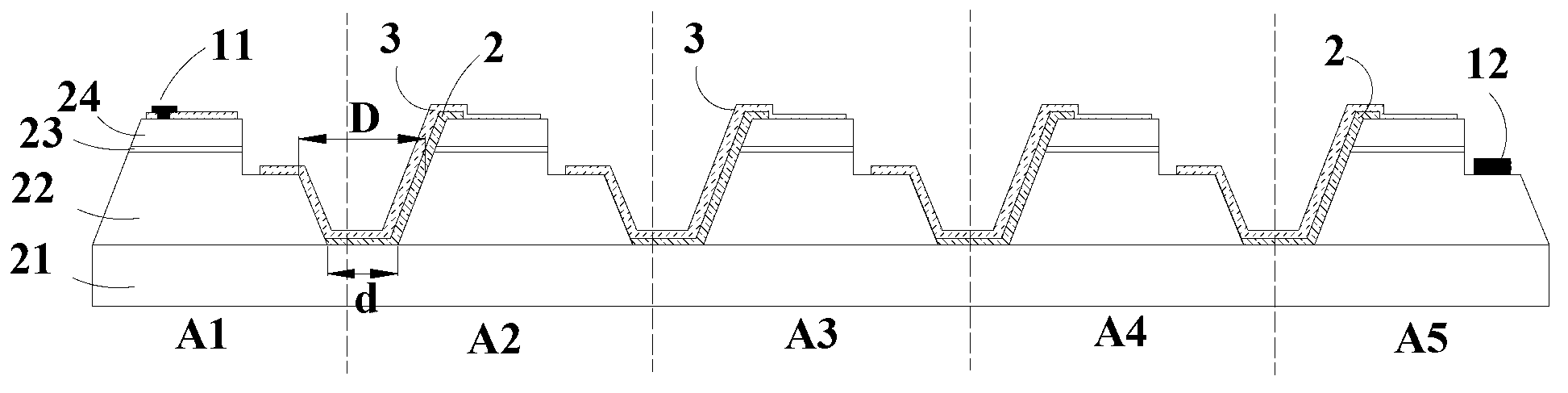
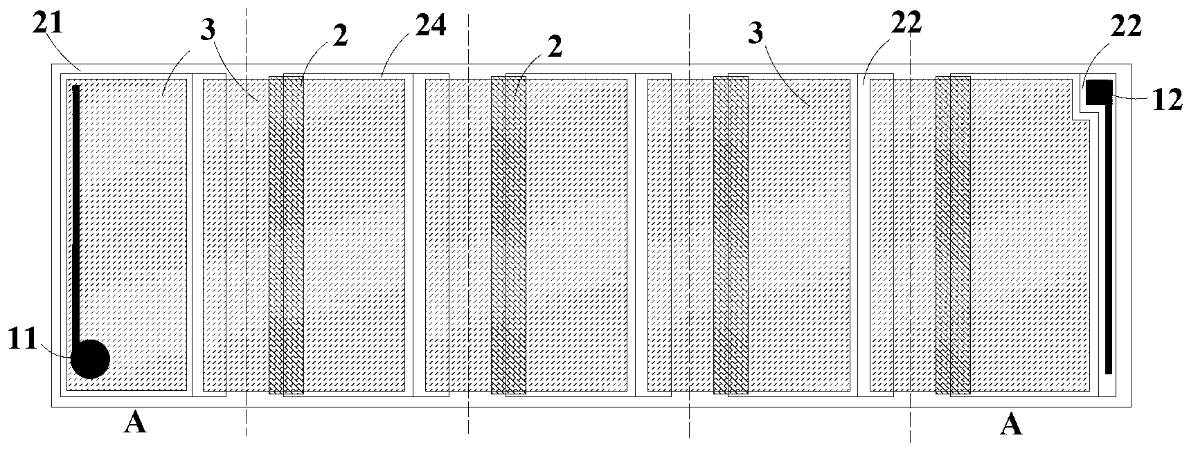
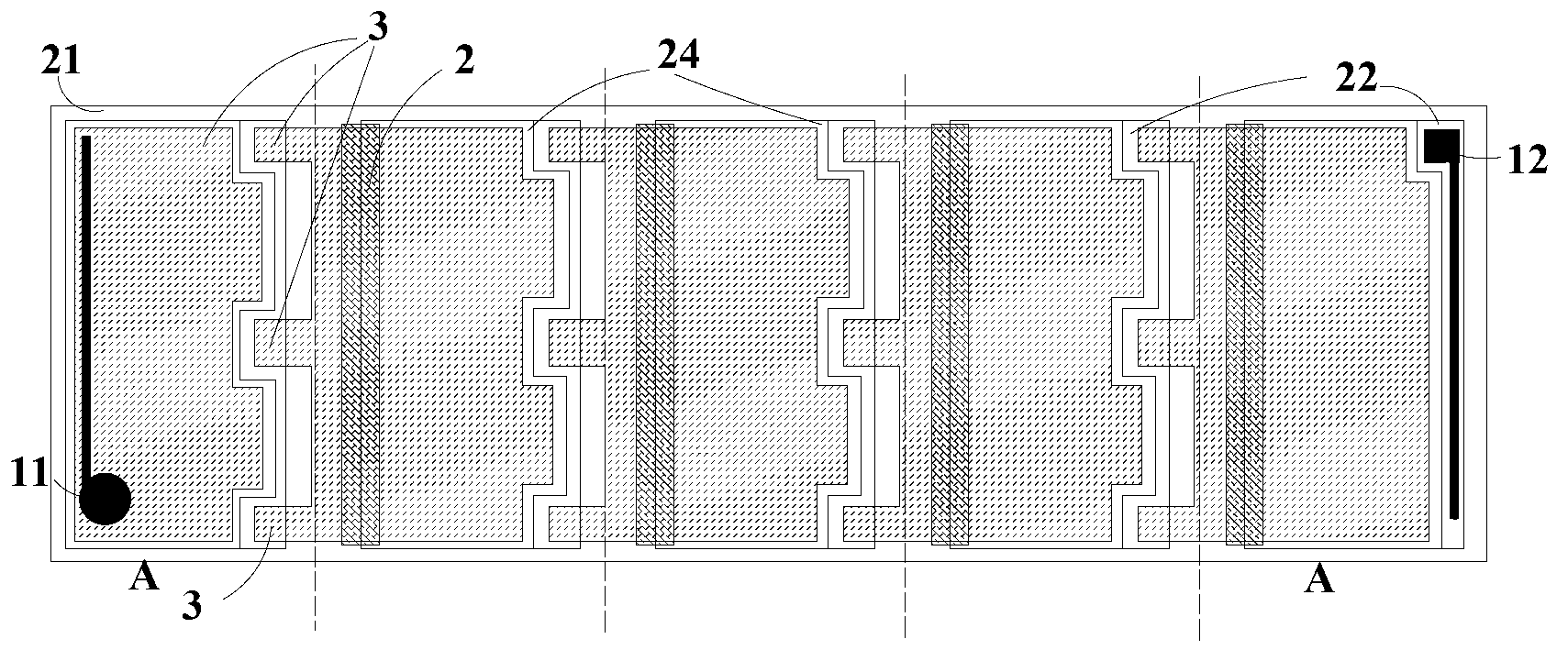
[0066] The invention provides a light emitting diode chip, comprising: a growth substrate, more than two light emitting diode units, deep trench isolation, non-metal wires and metal electrode pads, the light emitting diode uni...


PUM


Abstract

The invention provides a light emitting diode chip and a production method of the light emitting diode chip. The light emitting diode chip and production method of the light emitting diode chip comprise a growing substrate. More than two light emitting diode units are formed on the growing substrate. Each two adjacent light emitting diode units are separated by a deep groove. Non-metal wires are coated on the deep grooves. Two adjacent light emitting diode units are connected in series or in parallel through the non-metal wires. Metal electrode bonding pad is formed on a light emitting diode unit which is on the outmost periphery of the light emitting diode chip. The non-metal wires are adopted by the light emitting diode chip as an interconnecting structure among the light emitting diode units. Compared with metal wires which are high in thickness and poor in light-admitting quality, the non-metal wires are better in light-admitting quality and relatively thinner. When the light emitting diode chip is driven by high pressure, failure of the chip caused by fusing at the corner of a step is not prone to occur. Effective bright dipping area is enlarged and stability of the light emitting diode chip is improved.

Description

technical field [0001] The invention relates to a light-emitting diode chip structure and a manufacturing method, in particular to a light-emitting diode chip with a light-emitting diode unit and a manufacturing method. Background technique [0002] With the advancement of technology and efficiency, the application of light-emitting diodes (LEDs) is becoming more and more widespread, and with the upgrading of LED applications, the market demand for LEDs is also towards higher power and higher brightness - also known as The direction of high-power LED development. [0003] For the design of high-power LEDs, most major manufacturers currently use large-size single low-voltage DC LEDs. Large-size single low-voltage DC LEDs generally adopt two structures: one is the traditional horizontal structure, and the other is the vertical conductive structure. . [0004] The manufacturing process of the horizontal structure is almost the same as that of the general small-sized grains, s...

Claims


Application Information

Patent Timeline
Patent Type & Authority Applications(China)
IPC IPC(8): H01L27/15H01L33/62H01L33/00
Inventor 金豫浙张昊翔封飞飞万远涛李东昇江忠永
Owner HANGZHOU SILAN AZURE
Why Eureka
Try Eureka