Circuit board connection structure

A technology for connecting structures and circuit boards, applied in the structural connection of printed circuits, printed circuit components, etc., can solve the problems of PCB thickness, inability to achieve, and high implementation costs, and achieve thin thickness, small size, and fewer wiring layers. Effect

Active Publication Date: 2013-03-20
HUAWEI TECH CO LTD
View PDF5 Cites 12 Cited by
  • Summary
  • Abstract
  • Description
  • Claims
  • Application Information

AI Technical Summary

Problems solved by technology

Due to the limitation of PCB processing thickness, when the system expands in size and needs to further increase the wiring capacity between boards, the single board needs to further increase the wiring layer, which will cause the PCB to be too thick, and the implementation cost is high, or even impossible.

Method used


Image

  • Circuit board connection structure
  • Circuit board connection structure
  • Circuit board connection structure

Examples


Embodiment Construction

[0027] In order to make the object, technical solution and advantages of the present invention clearer, the present invention will be further described in detail below in conjunction with the accompanying drawings and embodiments. It should be understood that the specific embodiments described here are only used to explain the present invention, not to limit the present invention.

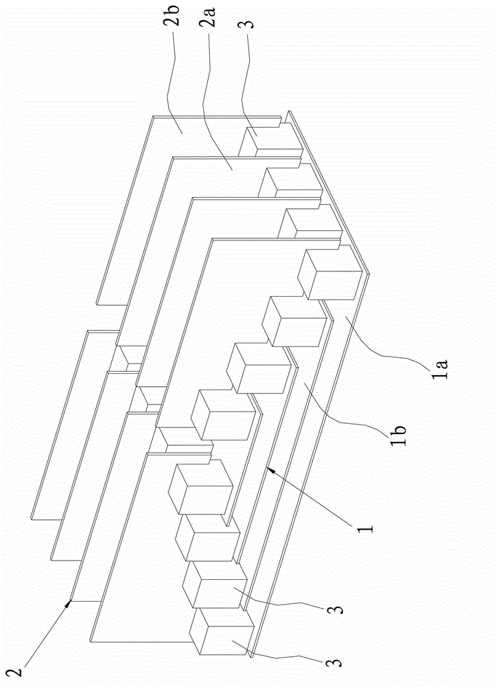
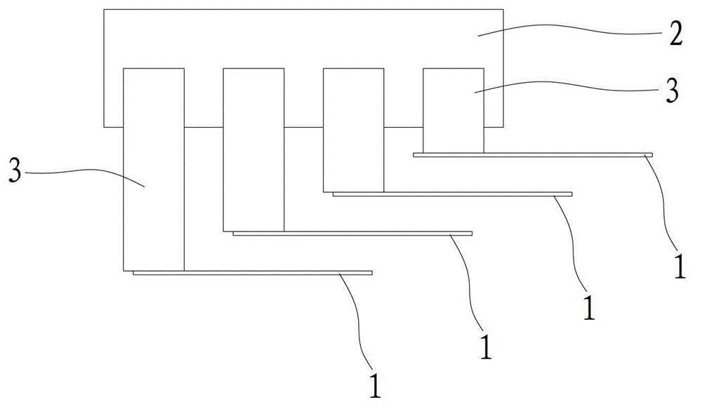
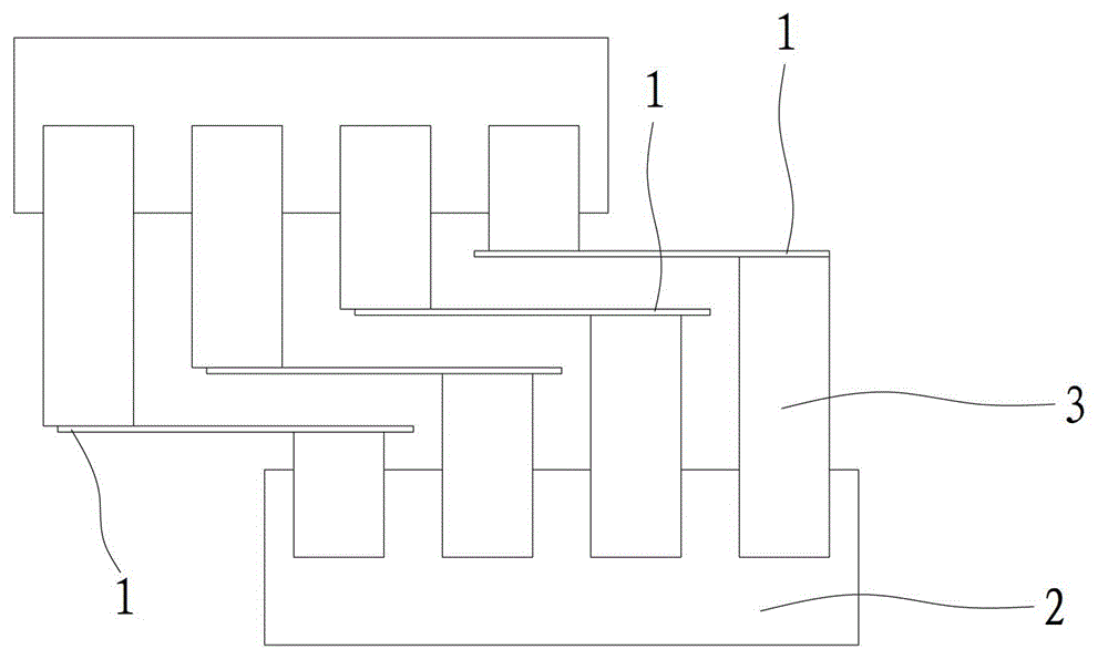
[0028] Such as figure 1 and figure 2 As shown, the circuit board connection structure provided by the embodiment of the present invention can be applied to large-scale equipment. The above-mentioned circuit board connection structure includes a sub-board 2 and at least two motherboards 1 stacked in layers. The motherboard 1 and the sub-boards 2 may both be PCB (Printed Circuit Board, printed circuit board). The so-called motherboard, which is equivalent to the base board, has a large size and is used to connect two or more sub-boards. The sub-boards are integrated through the motherboard; Signa...


PUM


Abstract

The invention is applicable to the field of circuit board connection structures and discloses a circuit board connection structure which comprises a secondary board and at least two main boards arranged in a stacking mode. Electric connectors are fixedly arranged on the main boards, and the secondary board and the electric connectors on the at least two main boards are connected. According to the circuit board connection structure, a plurality of circuit boards are stacked on three-dimensional space, and the limit that the circuit boards are arranged on two-dimensional plane is broken through so that intersystem interconnection is achieved, and a large quantity of signals is communicated; the number of layers of printed circuit boards (PCBs) is small, the external sizes are reduced, the sizes of a single main board and a single secondary board are small, wiring layers are few, the thicknesses are small, complicated intersystem interconnection is flexibly achieved, and the relevant circuit boards are easy to process and achieve and low in costs; and besides, the circuit boards can be designed into independent modules, specific compositions of the stacked circuit boards can be defined and detached respectively according to application requirements, and the flexibility is good.

Description

technical field [0001] The invention belongs to the field of circuit board connection structures, in particular to a circuit board connection structure with good expandability. Background technique [0002] In large-scale system equipment, circuit boards include single boards (single circuit boards) such as sub-boards and motherboards; generally, multiple sub-boards are used or connected to the same motherboard to realize signal connections between multiple single-boards. The sub-board and the motherboard are PCB (Printed Circuit Board, printed circuit board). When there are many interconnection lines, it is generally realized by increasing the number of PCB layers. However, there are certain limitations when such a single PCB is interconnected between boards: [0003] On the one hand, there is a limitation on the number of PCB layers. When the number of PCB traces is large, if the PCB size is constant, it needs to be realized by increasing the number of PCB layers. Howev...

Claims


Application Information

Patent Timeline
Patent Type & Authority Applications(China)
IPC IPC(8): H05K1/14
Inventor 李健郑国兰肖聪图
Owner HUAWEI TECH CO LTD
Why Eureka
Try Eureka