Structure capable of avoiding cold solder joint of elements and method thereof

A component and virtual soldering technology, which is applied in the structural field of avoiding component virtual soldering, can solve the problems of component virtual soldering, component soldering feet are higher than the body, and achieve the effects of improving production efficiency, reducing costs, and reducing failure and maintenance probability

Inactive Publication Date: 2015-07-15
GUANGDONG OPPO MOBILE TELECOMM CORP LTD
View PDF6 Cites 0 Cited by
  • Summary
  • Abstract
  • Description
  • Claims
  • Application Information

AI Technical Summary

Problems solved by technology

[0003] The main purpose of the present invention is to provide a structure and method that can skillfully avoid the virtual welding of the components for the above-mentioned special components, and solve the problem that the welding feet of the components are higher than the body and easily cause the virtual welding of the components

Method used


Image

  • Structure capable of avoiding cold solder joint of elements and method thereof
  • Structure capable of avoiding cold solder joint of elements and method thereof
  • Structure capable of avoiding cold solder joint of elements and method thereof

Examples


Embodiment Construction

[0017] The present invention will be further described in detail below through embodiments in conjunction with the accompanying drawings.

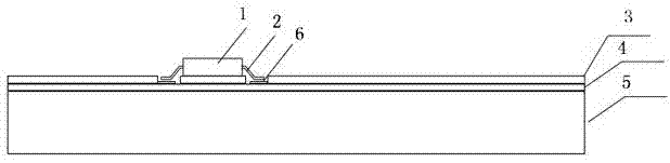
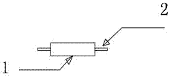
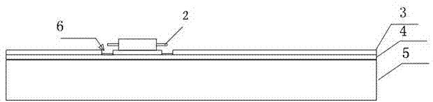
[0018] see Figure 4 , in some embodiments, the structure that avoids component false soldering comprises the PCB that is used for mounting component, and described PCB comprises base material 5, solder resist layer 3, copper foil layer 4 and the soldering pad that is arranged on copper foil layer 4 6. The solder pin 2 of the component is flush with the lower end of the component body 1 or higher than the lower end of the component body 1, and a sinking gap is opened at the part of the PCB corresponding to the lower end of the component body 1, and there is no obstruction in the sinking gap solder layer and copper foil layer. The sunken notch may also have no solder resist layer and the thickness of the copper foil layer in the sunken notch is smaller than the thickness of the surrounding copper foil layer 4, as long as the welding leg 2 ...


PUM


Abstract

The invention discloses a structure capable of avoiding cold solder joint of elements. The structure comprises a printed circuit broad (PCB) used for being pasted with the elements. The PCB comprises a solder resisting layer, a copper foil layer and welding pads arranged on the copper foil layer. Welding feet of the elements are aligned to the lower ends of element bodies or higher than the lower ends of the element bodies. A sunken notch is formed in a position, corresponding to the lower portions of the element bodies, of the PCB. The sunken notch is provided with no solder resisting layer or the copper foil layer inside, or the sunken notch is provided with no solder resisting layer and the thickness of the copper foil layer in the sunken notch is smaller than that of the copper foil layer on the periphery of sunken notch. The invention also discloses a corresponding method for avoiding cold solder joint of the elements. The problem that void-welding of the elements is easy to occur due to the fact that the welding feet of the elements are higher than the element bodies is effectively solved.

Description

technical field [0001] The invention relates to hardware electronics, in particular to a structure and method for avoiding false welding of components. Background technique [0002] In the SMT (Surface Mount Technology) materials used in the traditional process, compared with the component body, the solder feet of the component are generally flush with or slightly lower than the lower end of the component body, such as figure 1 shown. However, if figure 2 and image 3 As shown, for some special material components, the solder pin 2 of the component is higher than the lower end of the component body 1. Since the solder mask layer 3 and the copper foil layer 4 of the PCB (printed circuit board) have a certain thickness, the component body 1 is mounted on the solder mask layer. On layer 3, there is a height difference between the solder pin 2 of the component and the component body 1. When mounting, the solder pin 2 of the component is slightly higher than the pad 6 on the ...

Claims


Application Information

Patent Timeline
Patent Type & Authority Patents(China)
IPC IPC(8): H05K1/18H05K3/34
Inventor 刘建兵
Owner GUANGDONG OPPO MOBILE TELECOMM CORP LTD
Why Eureka
Try Eureka