Method for preparing a substrate by implantation and irradiation

一种衬底、注入粒子的技术,应用在半导体/固态器件制造、电气元件、电路等方向,能够解决劣化、不再具有最佳晶体矩阵等问题,达到减少光预算的效果

Inactive Publication Date: 2013-03-20
SOITEC SA
View PDF3 Cites 1 Cited by
  • Summary
  • Abstract
  • Description
  • Claims
  • Application Information

AI Technical Summary

Problems solved by technology

This poses a major disadvantage, since the surface of the sacrificial layer is degraded by these treatments, so it no longer has the optimum crystal matrix for epitaxy

Method used


Image

  • Method for preparing a substrate by implantation and irradiation
  • Method for preparing a substrate by implantation and irradiation
  • Method for preparing a substrate by implantation and irradiation

Examples


Embodiment Construction

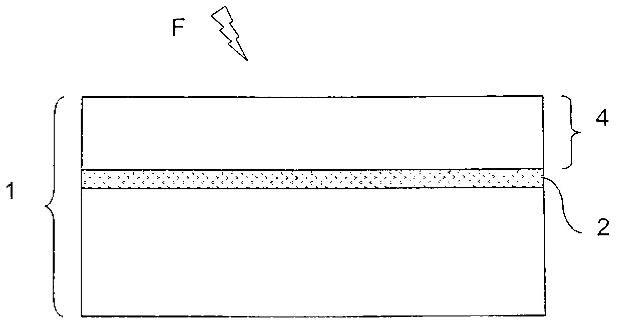
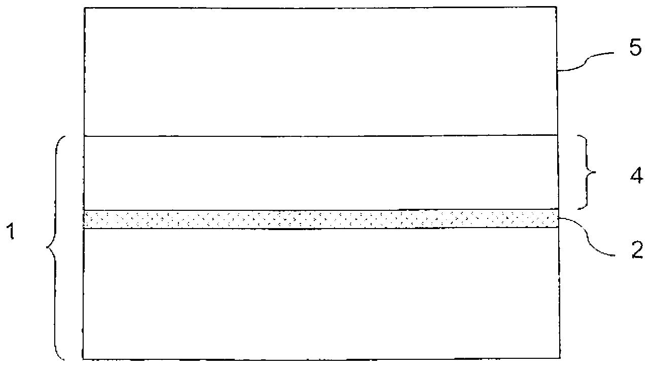
[0046] The present invention is applicable to any substrate made of crystalline or amorphous composite materials, the optical absorption properties of the composite materials (especially the optical absorption coefficient in the specified frequency range, or the imaginary part of the refractive index) can pass through the particles Inject and change in a local area. The composite material must also be able to decompose in the area under the influence of the energy input of the light flux in and near the area.

[0047] "Composite material" refers to a material composed of at least two elements.

[0048] "Decomposition" refers to a change in the basic structure of a material. Depending on the material, the change may consist of phase separation, generation of new phases, generation of inclusions, and the like.

[0049] Composite materials are materials composed of at least two kinds of atoms. Among the composite materials, III-V compound semiconductors, especially nitrides (ie, the g...


PUM

PropertyMeasurementUnit
absorption coefficientaaaaaaaaaa
diffusion coefficientaaaaaaaaaa

Abstract

The present invention relates to a method for preparing a substrate (1) with the purpose of detaching a layer, called the detachment layer, from said substrate by irradiation of the substrate with a light flux (F) for heating a buried region of the substrate and bringing about decomposition of the material of that region to detach said detachment layer, characterized by the fact that it comprises the steps consisting of: a) fabricating an intermediate substrate including a first layer (2) called the buried layer, and a second layer (4) called the covering layer, wherein the second layer (4) covers all or part of the first layer (2), the covering layer (4) is substantially transparent to said light flux (F), and the buried layer (2) which is formed by implantation of particles into the substrate can absorb said flux (F) for its part, and b) selectively and adiabatically irradiating a region called the treated region of the buried layer (2) until at least partial decomposition of the material constituting it ensues.

Description

Technical field [0001] The invention relates to a method for preparing a semiconductor material substrate, the purpose of which is to detach the layers of the substrate. Background technique [0002] III-N type semiconductor (with general formula Al x Ga y In 1-x-y N, where 0≤x≤1, 0≤y≤1 and x+y≤1), especially GaN, has characteristics that make it very attractive in the field of optoelectronics, power components and radio frequency applications. [0003] However, the development of these applications is slowed down by the technical and economic constraints of the substrate. [0004] In fact, device manufacturing usually relies on the transfer of a thin layer taken from a donor substrate to a support substrate, which is a bulk substrate of high-quality III-N material suitable for the desired application. [0005] In particular, Smart Cut TM The process is a well-known transfer technology, which usually consists of the following steps: implant a certain dose of atomic or ion species into...

Claims


Application Information

Patent Timeline
Patent Type & Authority Applications(China)
IPC IPC(8): H01L21/762
CPCH01L21/76254H01L21/762
Inventor M·布鲁尔
Owner SOITEC SA
Why Eureka
Try Eureka